Extreme ultraviolet (EUV) photoresist materials and processing are considered as one of the most critical issues in achieving the desired targets for EUV lithography. Extensive research has been conducted on high-performance photoresist materials,and recently numerous improved methods for photoresist processing have been reported. Photoresist development or dissolution is one such process that has been extensively studied, and it has garnered increasing attention over the past few years.
Various analysis methods, such as the quartz crystal microbalance and dissolution rate monitors,provide information that can help describe or defifine the behavior of a photoresist fifilm during the dissolution process. However, until now there has been no direct evidence of the mechanism operational on the photoresist fifilm during this chemical process. A visual observation of the actual pattern formation of photoresists during dissolution may provide new pointers concerning further improvement of the performance of the photoresist process.
Research on atomic force microscopy (AFM) has led to the development of ultra-fast scanning and nano-level analysis capabilities over the years. AFM measurements performed under a liquid solution have also improved and are already being applied in the dynamic observation of biomolecular processes.These continuous improvements in AFM capabilities indicate a remarkable potential in its application for the in situ analysis of the dissolution behavior of a photoresist.
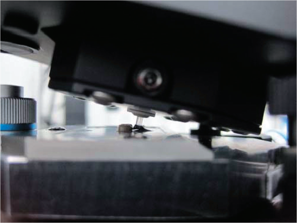
Figure 1 shows a picture of the high speed AFM (HSAFM) system (Nano Live Vision by Research Institute of Biomolecule Metrology), which is used here in the intermittent-contact mode. The HS-AFM system comprises a ‘‘sample assembly’’ to which a resist-coated and EUV exposed wafer sample is attached and a ‘‘cantilever assembly’’ where the cantilever and developer solution are set. An extensively improved version of the AFM reported in an earlier paper, the HS-AFM is equipped with highly sensitive, ultra-fast cantilever, and AFM scanning capabilities (temporal resolution: 80 ms/image).
The cantilever has a resonance frequency of approximately 1 MHz in water and a spring constant of 0.1– 0.3 N/m. An amorphous carbon tip was grown on the original cantilever tip by electron beam deposition. The tip length was adjusted to about 1μm, and the tip apex was sharpened by plasma etching (<15 nm in radius). A deflflection sensor is focused onto a small cantilever with an objective lens (20 times magnifification). For the analysis, an approximately 2x 2 mm2 wafer sample is set on a sample stage made of quartz glass. All HS-AFM measurements were performed at room temperatures.

Fig1
The wafer samples were prepared using the small fifield exposure tool (SFET, numerical aperture = 0.3).The SFET was linked to a coater/developer track system (Tokyo Electron Clean track ACT12) in a chemically controlled environment. The standard illumination condition used for the evaluation of the photoresist materials was an annular illumination of ☌outer 0.7/☌inner 0.3. The 32-nm isolated line (I/L) pattern exposures were made on a 300-mm ψ silicon wafer, which was then cleaved to obtain the 2 x2 mm2 wafer samples used for the in situ analysis. To obtain reference images of the SSR5 under standard photoresist processes, S-9380II (Hitachi High-Technologies) scanning electron microscope (SEM) for the top view and S5000 (Hitachi High-Technologies) for the cross-section view was utilized at optimal conditions.