The photothermal deflflection technique is applied in transverse confifiguration to measure the thermal diffusivity of semiconductor wafers. The large size of these samples inhibits the possibility to make the probe beam skim the sample at a small height which is required for a direct thermal diffusivity measurement. To overcome this problem, three new experimental schemes are proposed, each one based on a different geometry of the heat diffusion (one-, two-, or three-dimensional scheme).In particular for the 3D experimental scheme, a new mirage setup is described which uses two crystalline prisms 6 mm apart from each other to let the probe beam skim 50±3μm high over the sample surface, with a spot size of 22 μm. The main advantages of this setup, here discussed, are the obtained low probe beam height which is, moreover, independent of the sample dimensions, and the cheap technology to produce the necessary high-quality prisms. The performances of the new schemes have been tested by comparing, for well-known semiconductor wafers (InSb, InAs, InP, GaAs, GaP, Ge, and Si), the experimentally measured thermal diffusivity with the values reported in the literature.
It is well known that the thermal diffusivity (conductivity) of semiconductors is an important thermophysical property for controlling crystal and epitaxial fifilm growth processes. Different photothermal techniques have been successfully proposed and applied for the study of electronic and thermal transport in bulk semiconductors,thin fifilms and electronic devices.
Among the various techniques, the photothermal deflflection ( "mirage effect" )is an excellent contactless method for the investigation of optical and thermal properties. The technique concerns the analysis of the deflflection from its original trajectory of a probe laser beam traveling in a medium with a thermally induced refractive index gradient. The physical mechanism is based on the propagation of the thermal waves produced by an intensity modulated laser beam which heats the sample front surface. These waves propagate according to the heat diffusion process both in the sample and in the air layer surrounding it, giving rise to a temperature rise distribution. The thermal waves are detected by means of a second laser beam (probe beam) crossing the heated region, which is deflflected by the thermally induced refractive index gradient.
The photothermal deflflection technique when applied in its transverse confifiguration, which uses the probe beam traveling at some fifixed height from the sample surface, offers a useful way to investigate opaque samples, as the majority of semiconductors. The main problem of this scheme (skimming scheme) is connected with the fifinite size of the probe beam. In fact, although the waste of the probe beam is placed just over the heated region of the surface, the spot size increases at the edges so that, to avoid the probe beam scattering, the probe beam height has to be increased. This problem becomes particularly relevant for samples with a size larger than the probe beam Rayleigh length and can affect strongly the mirage data, leading to an error in the thermal diffusivity determination.

Fig1
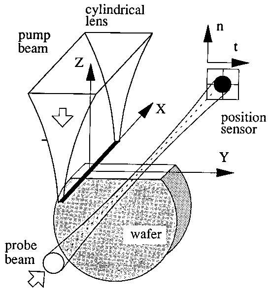
The request to perform photodeflflection measurements keeping the probe beam very close to the sample surface, has suggested us to let the probe beam to travel along the cleavage plane (see Fig. 1) of the wafer. The low thickness of the wafer, which usually is of the order of some hundreds of microns, compared to the probe beam Rayleigh length, allows one to adjust the probe beam in a vertical height of the order of the spot size without observing any diffraction pattern affecting the probe beam profifile.
As one can observe in Fig. 1, the pump beam is focused by a cylindrical lens in a thin line parallel to the probe beam direction and it is displaced laterally along the cleavage plane.10 In our experimental confifiguration the heat diffuses only along the yz plane (2D diffusion) and from the deflflection angle data the thermal diffusivity corresponding to the y axis can be found.
上一篇: 晶圆电互连应用的通孔制造技术比较
下一篇: 超声波振动对硅片抛光过程中材料去除的影响