Several techniques for fabrication of through-wafer vias in silicon have been compared in terms of achievable via diameter, shape and geometry and their influence on mechanical strength of silicon dies/wafers. Assessed techniques are: powder blasting, laser melt cutting, laser ablation, and deep reactive ion etching. The resolution of each method and influence on geometry was evaluated by fabrication through-wafer holes and slots in 240µm-thick silicon wafers. The mechanical strength is measured using ring-on-ring (RoR) and four-point bending methods. Additional stress-relief post-processing was applied to improve mechanical strength. Comparing performance of bipolar transistors before and after fabrication of laser ablated vias indicates that the electrically affected zone does not exceeds 10-20 µm around the via edge.
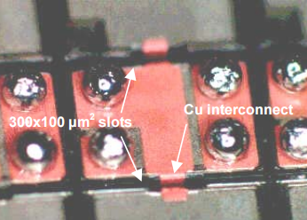
Application of through-wafer vertical interconnects for IC packaging may satisfy the needs of modern wireless communication products, which require more compact packaging solutions and efficient utilization of a footprint area, also referred as ‘silicon efficiency’. The throughwafer vertical interconnect provides smaller interconnect lengths resulting in lower parasitics and smaller propagation delays and is therefore highly attractive in RF packaging. Figure 1 shows just another application where through-wafer interconnect in a silicon substrate is utilized to demonstrate a wafer-level packaged, SMT-compatible power transistor.
The key technology for through-wafer vertical interconnects is fabrication of through-wafer vias. There are many different techniques that can be used for through-wafer via fabrication (see Table 1). Selection of a particular one depends primarily on the intended application and the substrate material. Not only the basic process parameters like achievable via dimensions, sidewall geometry, alignment accuracy, processing compatibility, throughput, etc. are of importance. When through-wafer vias are applied to fragile substrates like silicon wafers, their presence will inevitably affect mechanical properties of the entire wafer and also each individual die. Obviously, the mechanical strength of silicon wafer/die is weakened by the presence of through-wafer vias, especially in the case of high-density interconnects. The characteristics of employed techniques, resulting in different geometry of the fabricated vias (e.g. side-wall shape, surface roughness) and possible damage introduced into the silicon substrate (e.g. cracks, stress due to melting and subsequent solidification, etc.), can have a strong influence on the mechanical stability of the silicon wafer or die.
In this paper, four via-fabrication techniques, namely powder blasting, laser cutting, laser ablation and deep reactive ion etching are compared in terms of their influence on the mechanical strength of a silicon die, using ring-on-ring (RoR) and four-point bending methods. The electrically affected zone around laser ablated vias has also been evaluated by comparing the bipolar transistor characteristics before and after via fabrication.

Fig1
From the range of available techniques for fabrication of through-wafer vias in silicon (Table 1), following techniques were selected as capable to meet these requirements: powder blasting, laser ablation, laser melt cutting, and deep reactive ion etching (DRIE). The chemical etching, milling and mechanical drilling techniques were excluded from investigation, as only capable to produce vias larger than 150- 300 µm.
The laser cutting was done using Nd:YAG laser (further YAG) with wavelength of 1064 nm with pulse duration of 0.2 ms and spot size of 30-100 µm. The high-pressure gas flow removed the silicon melt downwards through the rigid support containing holes at the via-positions. ‘Burr’ is therefore located at the bottom-side of the wafer.
The ablation process works with frequency-tripled Nd:YAG laser (further 3YAG) with wavelength of 355 nm and short focused pulses of very high energy density to completely evaporate material with a negligible amount of melt. The spot size was as small as 10-30 µm with pulse duration of 30 ns to achieve the power density of 108 - 1010 W / cm2 . Both laser processes are maskless and PVA layers have been deposited on all wafers to prevent the wafer surface from contamination by the ejected material.