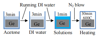
In this paper, we worked on development of cleaning solution for Ge surface and characterization from the electrical point of view. Samples supplied from two companies (Umicore and TDY Corporation) were cleaned by three different cleaning solutions (HF, HCl, and mixed HF-HCl), and subsequently heated by an electric furnace. Carrier mobility and bulk carrier concentration were measured by Hall system and compared these values for different samples. Cleaning by HCl gives better performance than HF and mixed HF-HCl solutions.
Semiconductor materials has many applications in modern devices because their electrical properties can be easily changed by adding impurities and silicon (Si) substrate is commonly used for these applications. However, the scaling of advanced MOS devices is approaching its technological and fundamental limits. Because continuous reduction in the process technology and gate length causes leakage current flows through the gate and mobility deration problems in the substrate. Therefore, new high-k material and high mobility substrates are mandatory.
Many researchers have found several candidates of high mobility channel material including germanium (Ge). Ge offers higher hole and electron mobility than Si, and has good affinity with Si. In order to fabricate the devices on Ge, surface contaminants should be in minimum levels with minimal increase in surface roughness.
There is well established cleaning method for Si surface. For Ge surface cleaning, scientists have applied various chemicals to remove contaminants as well as used different equipment to measure surface roughness. Till now there is no widely accepted cleaning method for Ge surface.

Fig1
Electrode is formed on cleaned wafer for further measurement and Titanium nitride (TiN) is suitable for making Ohmic contact in and N2 gases of 30 and 0.1sccm respectively are introduced when the chamber was pumped down to vacuum level. After addition of these gases, set pressure to 6Pa with RF power 200W for 1min 30sec to grow 27nm of TiN on Ge samples. TiN was developed close to the four corners by the help of a metal mask that had four holes (Fig. 2a). For better probe connection and measurement, aluminum (Al) is deposited on TiN position because the grown TiN is hard and is done by evaporation technique after placing small Al pieces into the evaporator. The machine is turned OFF, once 200nm thick Al is deposited on TiN (Fig.2b).
Samples that experienced chemical cleaning and heating are placed into a Hall system, and obtained data from electrical point of view. The measured data contained different parameters. Among them, mobility and bulk carrier concentration are important because others can be calculated by putting these values into numerical equations and comparison of these values between samples gives the impact of different cleaning solutions. Data are measured for one pair of samples without cleaning and referred to as ‘As received’, and is used to compare with the data that obtained after cleaning. Fig.3 and 4 shows the majority carrier mobility and bulk carrier concentration for Umicore and TDY samples respectively.
Three different chemical solution was employed for Ge surface cleaning and found HCl solution brought better impact for Ge cleaning in terms of mobility and carrier concentration regardless of the samples provided by two companies.
上一篇: 超声波振动对硅片抛光过程中材料去除的影响
下一篇: 声电化学参数在半导体清洁中的作用