The electronic effffects of semiconductor doping pose a unique challenge for fifirst-principles simulations, because the typically low concentration of dopants would require intractably large system sizes in an explicit atomistic treatment. In systems which do not display longrange band bending, a satisfactory remedy is offffered by the use of “pseudoatoms”, with a fractional nuclear charge matching the bulk doping concentration. However, this alone is insuffiffifficient to account for charged semiconductor surfaces in the general case, where the associated space-charge region (SCR) may be very wide relative to tractable simulation dimensions. One generalization of the pseudoatom approach which overcomes this diffiffifficulty relies on the introduction of an artifificially high doping level within a slab calculation, in conjunction with a multi-scale electrostatic energy correction. Here, we present an alternative technique that naturally extends the pseudoatom approach while bypassing the need for calculations with an unrealistically high doping level. It is based on the introduction of a two-dimensional sheet of charge within a slab-based surface calculation, which mimics the SCR-related fifield, along with free charge such that the system is neutral overall. The amount of charge involved is obtained from charge conservation and Fermi level equilibration between the bulk, treated semi-classically, and the electronic states of the slab/surface, which are treated quantum-mechanically. The method, which we call CREST - the ChargeReservoir Electrostatic Sheet Technique - can be used with standard electronic structure codes. We validate the approach using a simple tight-binding model, which allows for comparison of its results with calculations encompassing the full SCR explicitly. Specififically, we show that CREST successfully predicts scenarios spanning the full range from no to full Fermi-level pinning. We then employ it with density functional theory, where it is used to obtain insights into the electronic structures of the “clean-cleaved” Si(111) surface and its buckled (2x1) reconstruction, at various doping densities.
Semiconductor doping, which entails the introduction of impurities at concentrations typically of the order of parts per million, is of immense physical and technological importance. Beyond its extensive intentional use in semiconductor technology, many semiconductors (e.g., GaN or ZnO ) often possess unintentional native defects that result in an effffective doping which cannot be ignored. While such impurities/defects affffect the chemical and crystalline properties of the bulk only locally, they dominate the electronic properties globally by increasing the amount of free charge carriers of either polarity, possibly by many orders of magnitude above the pristine semiconductor’s intrinsic (thermally excited) concentration. This increase in charge carrier concentration is reflflected in a shift of the Fermi level (EF ) position (typically) in the semiconductor forbidden gap .
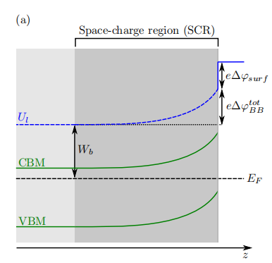
At semiconductor surfaces (or interfaces), the existence of gap states may cause charge transfer between the doped material and its surface. The (typically) resulting depletion of free charge carriers from the region adjacent to the surface creates a space-charge region (SCR) originating from spatially fifixed, ionized impurities. If the impurities are dilute, the SCR can extend hundreds of nm from the surface. The space charge creates an electric fifield which shifts the energy levels near the surface relative to their position in the neutral bulk, and thus relative to the global EF , which is fifixed by the bulk doping ratio and energy levels. For convenience, we use below the term “surface Fermi level” to indicate the position of EF relative to the band edges nearest the surface, which may diffffer from its position relative to the band edges in the neutral bulk (see, e.g., Fig. 1(a)).

Fig1(a)
We have found that this intersection-of-curves procedure is robust even if bulk-like conditions are not strictly achieved within the slab (which we deduce by observing that the slope of Ua(z), extrapolated from within the slab, diffffers from its slope in vacuum divided by the bulk dielectric constant). This typically creates only a minor deviation in the estimate of the slab’s “formal edge”, i.e., of zd. In our various numerical tests, described in detail below, we found that even an error as large as 2 ˚A in zd leads to no more, and usually much less, than a ∼5 meV error in the converged position of the slab’s Fermi level, which is the most sensitive slab parameter examined.
The atomistic slab is constructed by the user such that one side of the slab is the surface of interest and the other is a passivated, virtual surface, with “doped” semiconductor atoms within the slab. The charged sheet is placed to the left of the virtual surface, far enough from it such that no charge density is found in its vicinity (the exact position of the sheet does not affffect the physics, as long as periodic boundary conditions parallel to the surface are set). The user must also provide Wb and △ψv obtained from a calculation of the fully passivated slab (see Fig. 2), which only needs to be performed once for the entire self-consistent cycle.
上一篇: 异构集成 SOI化合物半导体光子学
下一篇: 掺杂磁性半导体中的谐振光伏效应