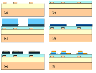
Silicon has been shown to be an excellent material for realising compact photonic integrated circuits (PIC) operating in the telecom wavelength range (1100nm- 1600nm). Crystalline silicon has very low intrinsic propagation losses and both large core fiber matched waveguides and extremely compact so-called photonic wire circuits have been demonstrated. Through carrier injection or depletion the real and/or imaginary part of the refractive index can be changed, allowing for switching and modulation of light. Since silicon is intrinsically transparent at these wavelengths, integration with other materials is required however for realizing efficient optical sources and detectors. The latter are now typically based on Ge, integrated with the silicon waveguides using heteroepitaxial growth techniques. Although being investigated intensively, these have had only limited success thus far for integrating compound semiconductors on silicon however, which is required for realizing compact light emitters and amplifiers. Therefore, several groups developed an alternative integration scheme, based on waferbonding technologies, which avoids the growth step but still allows for a process compatible with waferscale processing techniques. The latter is not only important from a cost perspective, but it also allows for accurate alignment of the active devices with respect to the underlying circuits. This paper reviews work of different groups in this field. In the following section the integration approach is described in more detail. Next, an overview of several fabricated devices is given.
A classic approach in integrating III-V semiconductor devices with silicon (and silica) PICs is based on flipchip bonding. In that case prefabricated optoelectronic devices (e.g. a DFB laser array) are bonded upside down on a suitable substrate (e.g. a recess in the PIC) . In some cases the substrate is largely removed before bonding . No or little comprises are required in the design of the optoelectronic devices and they can be pretested. Therefore, for small to medium volumes this is certainly an attractive route, although reaching the required placement accuracy (typically +/- 1um) is far from trivial and the interface can exhibit considerable loss. For large scale integration however, there is a need for an integration approach compatible with waferscale technologies as described above.

Fig1
The first electrically injected III-V on silicon lasers were demonstrated in 2006. Fabry-Pérot lasers were demonstrated using an approach whereby most of the light is concentrated in the III-V area of the laser section and coupled to the silicon waveguide through a polymer taper once exciting the laser facet. In a hybrid integration platform was demonstrated whereby most of the light is concentrated in the silicon waveguide and the mode is evanescently coupled to the waveguide region on top. This platform was rapidly extended to more complex laser designs. DFB-lasers as well as DBRlasers were demonstrated, with output powers of respectively over 4mW and over 9mW. In combination with quantum well intermixing (prebonding) for defining regions with different band gap also integrated sampled grating DBR-EAMs were shown. See for a recent review.
For short reach interconnect applications and alloptical signal processing however low power laser sources are required. Therefore we developed electrically injected microdisk sources, employing a whispering gallery mode in a III-V semiconductor disk structure. Initial devices had a threshold current of 0.5mA and where limited in output power . In recent devices, having an improved heat sink, the threshold current was reduced to 0.260mA and the output power (CW operation) increased to 0.120mW . These devices can also be used as electro-optic modulators , all-optical wavelength convertors or as part of a compact multi-wavelength laser .
Heterogeneous integration of compound semiconductors has proven to be a very powerful platform for realising efficient sources integrated with silicon waveguides. Further improvement will require new device structure, e.g. using photonic crystal structures for improved light confinement or new material types. Promising candidates are selfassembled materials such as colloidal quantum dots or compound semiconductor nanowires .
上一篇: 多层衍射光栅清洗方法的评价
下一篇: 掺杂半导体表面电子结构的多尺度方法