Maintaining low-defect spin-applied films is paramount to the success of semiconductor manufacturingWhile some spin-on films have a low number of defects as coated, defect levels can rise with the number oiwafers processed. Thin organic films may outgas or sublime during the post-coat baking process, or evenduring subsequent exposures to deep or extreme ultraviolet radiation. lf these outgassing componentscollect on the lid of the hot plate chamber, there is an increased risk of “fall-on defects on subsequentlorocessed wafers. To increase throughput, preventive maintenance and cleaning schedules are pushed to theimit to provide maximum output from the track. New materials must be designed to produce minimaoutgassing to ensure maximum throughput without defects. Early tests for measuring outgassing providedqualitative results gained from collecting the condensed outgassing components on a quartz wafer andmeasuring the absorbance of the resulting film. A more advanced technique involves the use of a newlydesigned quartz crystal microbalance (OCM) to more carefully quantify the amount of outgassing.As theindustry continues to mature. more sensitive measurements are reauired to design new materials with evenlower outgassing from sublimation. The combination of OCM and inverted wafer test provides an overallview of total outgassing and ramifications of the outgassing being produced.
Maintaining low-defect spin-applied films is paramount to the success of semiconductor manufacturingSignificant elfort has been placed on reducing defects of spin-on applied films by making improvements tomaterial formulations, application processes, and application equipment. A primary requirement for spinon films is to have a low number of defects as coated. Without a substantially defect-free coating, yieldand thus profits, will be reduced. An often-overlooked problem in early screening of materials is theoutgassing eflects on defect levels. Thin, organic films may outgas or sublime during the post-coat bakingprocess, or even during subsequent exposures to deep or extreme ultraviolet radiation. lf these outgassingcomponents collect on the lid of the hot plate chamber, there is an increased risk of fal-on defects onsubsequently processed wafers whereby defect levels can rise with the number of warers processed betweencleaning of the collection surface. Cleaning the collection surface alleviates this problem. To increasethroughput, preventive maintenance and cleaning schedules are pushed to the limit to provide maximumoutput from the track. New materials must be designed to produce minimal outgassing to ensuremaximum throughput without defects.
Early tests for measuring outgassing provided qualitative results gained from collecting the condensedoutgassing components on a quartz wafer and measuring the absorbance of the resulting film. A moreadvanced technique involves the use of a newly designed quartz crystal microbalance (OCM) to morecarefully quantify the amount of outgassing. As the industry continues to mature, more sensitivemeasurements are required to design new materials with even lower outgassing. Materials that formextremely thin coatings necessarily contain a high percentage of solvent and other volatile components thatwould be dificult to remove completely while retaining desired film properties. However. not alloutgassing collects and forms particles on a surface that can render a fall-on defect. To ensure a reduction infall-on defects without the convolution of benign evaporation, a combination oftesting is required.
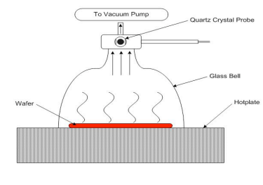
The OCM (Fig. 1) was developed for the purpose of determining the sublimation of samples of BARC andother spin-on coating products. The quartz crystal was suspended over a hot plate where it could collectthe outgassing from the wafer below. A ventilation line was attached at the top to draw airflow upwardsand allow the outgassing to condense on the surlace of the quartz crystal. The condensate collected on thecrystal, and the change in resonant frequency was corrected to mass units of the condensate. The standardprocess for measurement includes a 4-inch silicon wafer coated with an organic spin-on coating. The waferwas then placed under the OCM on a hot plate at 205°C for 120 seconds. The data were collected andgraphed to show sublimate versus time.

The OCM graph in Fig. 3 shows that the total output of outgassing of catalyst 1 and catalyst 3 wasapproximately 1800 nanograms of sublimate each, whereas catalyst 2 sublimed at a higher rate to produce2200 nanograms of sublimate. In Fig. 4, catalyst 1 and catalyst 2 sublimed at higher rates to produce2200 nanograms each compared again to catalyst 3, which produced 1800 nanograms of sublimateCatalvst 3 performed the best with both crosslinker formulations. Catalyst 2 was similar in maintaining ahigher sublimation rate for both crosslinkers. Catalyst 1 exhibited an interesting difference between thecrosslinkers. Combined with glycouril. catalyst 1 produced outgassing comparable to that of catalyst 3Combined with melamine, catalyst 1 produced a higher amount of outgassing comparable to that of catalyst2. The OCM is mass sensitive and cannot distinguish between a residue, a partial film, or large particlesThe quartz crvstal measures only the material that has adhered to the surface of the crystal. The OCNcannot distinguish among polymer, crosslinker, PAG, TAG, quencher, and/or solvent system outgassing; itmeasures only the total collection of the mass condensed. The OCM system helps in the first line ofdetection of possible future problems by helping to keep the outgassing of new formulations at reasonablelevels.
上一篇: 掺杂磁性半导体中的谐振光伏效应
下一篇: 激光冲击波对阳极氧化物半导体界面的影响