In contrast to silicon, intrinsic oxides have not been widelyused to protect compound semiconductors-based devicesyet. An anodic oxide(AO) seems an exclusive example, andit is used to passivate HgCdTe (MCT) based photocon-ductive detectors. However, AO-based structures havepoor thermal stability. At temperatures above 100 C a ntype layer is formed at a semiconductor interface, with thickness and carrier concentration increasing up to a certainvalue as temperature and annealing durationincreasing 3.4.HgZnTe-based AO structures(5, 6 demonstrate betterthermal stability, but current state of the art does not allowto fabricate high-quality material for wide application. Thatis why techniques to control interface characteristics andAO-MCT structures thermal stability should be developedThe laser shock wave (LSW) treatment could be an ad-equate approach.
Recently we havestudied theLSWimpact on bulk MCTsingle crystals both n- and p-type. The results we obtained show that LSW-induced gettering ofnative pointdefects on different sinks is a major contributor that is in agood agreement with. Since properties of crystals with macroinhomogeneties were themost changed, we can expect parameters ofthe AO-MCT interface with its well knownstructure to be changed considerably as well.
Neodymium-glass laser pulses with 1.06 mm wavelength30 ns pulse width, were used to induce a shock wave in thesamples atroom temperature. A 100 mm copper foil wasused as an opaque overlayer to protect samples from thethermal influence of the laser beam. Dimensions ofsamplesto be treated were chosen to assure the shock compressionto be uniform and uniaxial (typical dimension is 5x6x1 mm3).
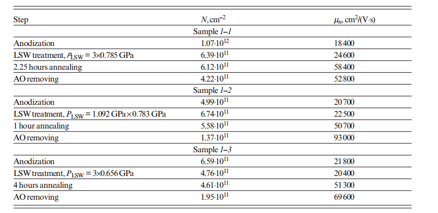
Three groups of samples were studied. The processingsequence used in experiments with the group / samplesincluded anodization and annealing in ambient air at 150 Cimmediately after anodization without LSW treatment. Incontrast, the group 2 samples were annealed under the sameconditions after anodization and ISW treatment ofthe back(not oxidised) sample surface. And finally the group 3 sam-ples were treated in the following way - anodization, LSWtreatment (LSWenters the anodized surface) and anneal-ing as it is described above.

Fig1
Hence, newly formed complexes enlarge the inducedcharge. We suggest pressing back the mobile charge intothe oxide bulk to be highly probable, and both the increaseand decrease ofthe residual charge can happen dependingontheremoved - generated charge relation as it was foundout with galvanomagnetic measurements. Secondly, suchcomplexes prevents the elemental mercury from diffusingfrom thelayer above. It is mainly due to moving the elemen-tal mercuryfrom the interfacethat the post-annealing electron concentrationin LSW-treated samples is less than thatin samples which were not exposed to LSW. Thereis a certain decrease of the fixed charge after annealing that maydecrease the measured electron density. On our opinionthis can be explained by oxygen indiffusion resulting in fillingoxygen vacancies in complexes responsible for the fixedcharge. Forannealing in the ambientair, Augerspectra indi-cate an increased oxygen content at the interface.