This paper reviews the recent progresses obtained by direct growth of III–V semiconductor quantum dots (QDs) on prepatterned and flflat silicon substrates. This combination allows us to study in detail the growth mechanisms of III–V materials on silicon substrates. For the flflat surfaces, we concentrate on basic growth studies addressing mainly morphological properties of QD-like structures with a main emphasis on surface preparation and growth parameters. For the pre-patterned substrates, we report the optimization of electron beam lithography and dry etching processes to fabricate sub-100 nm holes in prepatterned Si (100) substrates with controlled size, shape, and periodicity. The pre-patterned silicon substrates underwent thorough ex situ chemical and in situ cleaning processes before the molecular beam epitaxy (MBE) growth. Finally, the MBE growth sequence of QDs on patterned silicon surface has shown highly selective formation of localized dome like nanostructures in patterned holes with 1mm period.
Silicon is the main material for various semiconductor devices with approximately 90% of the semiconductor industry. However, indirect nature of the silicon band structure prevents the realization of effificient light emitting devices. On the other hand, III–V materials, due to their excellent optical properties and optoelectronic capabilities, are widely utilized in conventional photonic devices such as lasers and LEDs. Integration of III–V semiconductor compound light sources with silicon is highly sought for the realization of photonic integrated circuits using the well-established complementary metal-oxide-semiconductor (CMOS) fabrication technologies. In particular, optical interconnect systems provide a promising approach for the realization of the next generation high-speed communication and computing technologies.
In contrast to the III–V/IV systems, tremendous progress in the growth of In(Ga)As quantum dots (QDs) on prepatterned GaAs substrates has been made . Sitecontrolled In(Ga)As QDs with very narrow linewidth photoluminescence signal have been achieved both in inverted pyramidal and round-shaped nanoholes . A detail of specifific lithographic process for the prepatterning of silicon surface with sub-100 nm holes for the MBE overgrowth has not been reported explicitly in the literature as the site-controlled growth of QDs on silicon is a relatively new fifield. Therefore, we have carried out considerable work in order to develop and optimize an etching process suitable for the purpose of over-growth on pre-patterned silicon. In recent years, some research efforts have also been made to realize the growth of III/V QDs on pre-patterned silicon substrates using SiO2 as a mask which show encouraging results. For such fabrications, several lithographic techniques are in use for pre-patterning silicon substrates, such as focused ion beam (FIB), scanning probe techniques and electron beam lithography (EBL). However, the EBL is the most widely used technique to fabricate features even in sub-10 nm range.

Fig1(a)
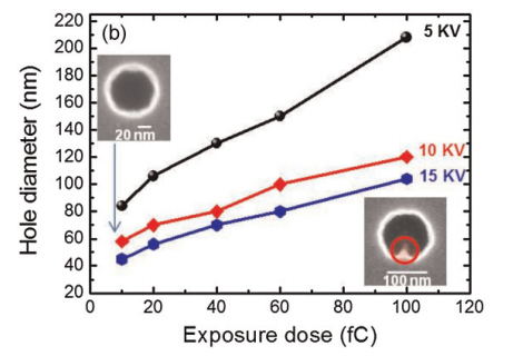
For a given beam acceleration voltage the diameter of the patterned hole increases linearly with the exposure dose due to beam spreading caused by increased generation of secondary electrons and their scattering through the resist (Fig. 3b). The holes patterned with smaller exposure dose (10 fC) have around 60 nm diameter in size and well defifined round shapes whereas those with high exposure dose (100 fC) have traces of carbon contamination (indicated by a red circle in the inset of Fig. 3b) due to the carbonization of PMMA resist . Low exposure dose (10 fC) was thus selected for the patterning of nanoholes on silicon.
The control over the hole diameter was achieved by increasing the dose for a single pixel exposure. Figure 3a shows the impact of increasing the exposure dose over the hole diameter for a given e-beam acceleration voltage. The hole diameter increases almost linearly with increasing exposure dose. This can be explained in terms of enhanced forward scattering with increasing exposure dose which results in an enlargement of the hole diameter. The inset of Fig. 3b at a dose of 100 fC shows the emergence of traces of carbon contamination in the fabricated holes for enormously high exposure doses indicated by the red circle. Such a situation occurs when hydrogen and oxygen bonds with carbon are broken and subsequent evaporation of hydrogen and oxygen takes place leaving carbon behind. Hence very high exposure doses have to be avoided for single pixel dot exposure.
上一篇: 激光冲击波对阳极氧化物半导体界面的影响