The RCA cleaning processes has been used for more than 30 years in silicon cleaning processes.1 It is still used in advanced complementary metal oxide semiconductor (CMOS) production lines. There are two steps in the RCA cleaning process. The fifirst step is using an NH4OH:H2O2 :H2O mixture (namely, standard clean 1, SC-1)! to remove particles and some trace metallic contamination. The second step is using an HCl:H2O2 :H2O mixture ( namely, standard clean 2, SC-2) to remove metallic contaminants. The temperature of both steps are ; 70°C, and the exposure time is 10 min. Generally, if wafers undergo patterning and stripping processes involving the photoresist ( PR) before the standard RCA cleaning process, an additional step including H2SO4 :H2O2 (SPM) should be added to remove the residual PR. In standard CMOS processes, many different cleaning processes must be used to maintain cleanliness on the wafer surface during the whole process. Figure 1 shows a typical cleaning process in a deep subquarter micrometer CMOS fabrication. It can be seen that before silicidation, generally referred as the front-end processes, there are 19 cleaning steps. It is noted that four different cleaning methods are used. Clean A consists of SPM followed by RCA. Clean B consists of the RCA. Clean C consists of SPM only. Clean D consists of SPM followed by diluted HF solution (pregate oxide cleaning) . Obviously, the number of cleaning steps in a typical CMOS fabrication process is large and cleaning methods are complex at the same time. Recently, many modififications of the conventional RCA two-step cleaning process have been proposed for improving cleaning effificiency and to reduce process cost and cycle time.2-5 However, these reports focus only on the pregate oxide cleaning (clean D) . The purpose of this paper is to present a one-step single-solution cleaning process to replace all cleaning methods mentioned above and listed in Fig. 1. The cleaning effificiency and the performance of the fifinal devices is shown to be comparable to RCA counterparts.
Particle numbers on the wafer surface were measured by a Tencor surface model 4500 system. The surface roughness was measured by atomic force microscopy (AFM) , while metallic contaminants were anon n-MOSFETs were measured by a Hewlett-Packard (HP) 4156 semiconductor parameter analyzer. The flflatband voltage and interface trap density were obtained by Keithley C-V system.alyzed by total reflflection X-ray flfluorescence spectrometer (TXRF, Rigaku model 3700) . Electrical measurements .
Another important concern for the interconnect ( IC) industry regarding the conventional RCA cleaning process is the required huge amount of DI water consumption. Since two cleaning steps are required in each RCA cleaning process, two DI water rinsing cycles are needed to remove the residual chemicals on the wafer surface. In Table I, we compare the DI water consumption and processing time for both methods. Based on the CMOS logic processes shown in Fig. 1, a CMOS lot requires four different cleaning methods. Each of the four cleaning methods ( i.e., clean A, B, C, and D) requires 3, 2, 1, and 1 DI water rinse cycles, respectively, as shown in Fig. 1. In contrast, only one DI water rinsing step is needed when using the one-step cleaning method. A 20 times reduction in DI water rinse cycle is achieved by using the new one-step single-cleaning solution in the CMOS processes. The typical processing time saved for cleaning steps is also estimated and shown in the fifigure. The total cleaning time required(which includes both cleaning and DI water rinsing times) for clean A, B, C, and D are estimated to be around 60, 40, 20, and 50 min, respectively. The total saving in time is estimated to be around 8.75 h for each lot by adopting the one-step cleaning method.

Fig1
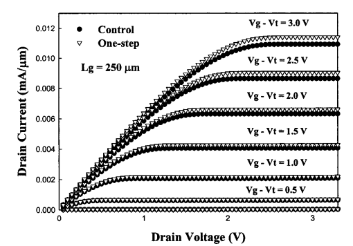
In this paper, we have demonstrated a new one-step cleaning recipe for CMOS fabrication. In this method, the one-step single solution is used to replace the conventional RCA two-step cleaning method in the entire CMOS processes. The results of the n-MOSFETs from two split lots show comparable, or even better performance for the new one-step recipe. The potential benefifits which are signifificant for the IC industry include shorter cleaning time, less DI water and chemical usage, and shorter cycle time for CMOS processes. It also benefifits our environment by reducing chemical waste.