The impact of metal–oxide–semiconductor processing on strained Si/SiGe device structures has been examined. Material was grown by gas-source molecular beam epitaxy and ultra low pressure chemical vapor deposition, with different as-grown surface roughness. The effects of RCA cleaning, gate oxidation and rapid thermal annealing on this material were studied by atomic force microscopy (AFM) and optical profifilometry. Certain processes caused reactions common to both material types, whereas others yielded dissimilar responses. Filtering AFM roughness data of specifific wavelengths enabled the effects of processing on large-scale surface roughness dominated by the cross-hatching morphology and smaller scale microroughness to be investigated. The results suggest that as-grown Si/SiGe material quality is not a good indicator of processed device performance, rather morphological changes which occur during processing must be considered.
In 1965, Gordon Moore successfully predicted that the performance of integrated circuits would double every 18–24 months. This prediction has largely been achieved in complementary metal–oxide–semiconductor (CMOS) technology through the aggressive scaling of device dimensions and in particular, an exponential decrease in transistor gate length with each technology generation. While further performance enhancements remain possible using current Si technology, increasing design and fabrication costs for new technology generations may make them prohibitive.1 Thus, alternative materials with advanced properties for mainstream applications are actively being sought. The Si/SiGe material system is presently receiving widespread attention due to its successful integration into bipolar technology2 and, with its incorporation into CMOS technology, the promise of even greater performance advantages compared with conventional Si without the high costs associated with geometric scaling. The clear benefifit of the strained Si/SiGe system compared with other advanced material systems is its compatibility with conventional Si fabrication techniques. This has recently led to the addition of strained Si/SiGe as a key emerging research technology in the 2001 International Technology Roadmap for Semiconductors.
While theoretically predicted mobilities have been demonstrated experimentally in strained Si/SiGe n-channel heterojunction modulation-doped fifield-effect transistor (MODFET) structures operating at room temperature,6 the performance of strained Si/SiGe n-channel heterojunction MOSFETs (HNMOSFETs) fabricated on both gas-source molecular beam epitaxy (GS-MBE)material7 and chemical vapor deposition (CVD) material8 has been somewhat lower than in theory. Since MODFET devices require far less processing than MOSFETs, the degradation in HNMOSFET performance appears to be caused by device fabrication, and in particular, the difference between MOSFET and MODFET processing.

Fig2
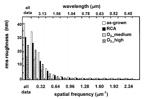
The results in Fig. 2 show the effect of processing on the average rms roughness in bands of 5% of the total frequency range probed by AFM from all the 40x40 μm² areas measured on the GS-MBE samples. At each frequency band resolved, there was a reduction in roughness following RCA cleaning. The average rms roughness from all the AFM areas analyzed was found to decrease by 30% following cleaning. Moreover, the variation in roughness decreased by over 50% in terms of the standard deviation of the mean value compared with roughness measurements on as-grown material. The ULPCVD material showed a similar trend. The average as-grown rms roughness was reduced by 20% following RCA cleaning, and the variation in roughness was reduced by approximately 60%.
The samples of ULPCVD material subjected to RTA were used to investigate whether the enhanced microroughness was caused by high temperature or from the oxidation process itself. The morphology of the annealed samples was found to degrade in the same manner as the oxidized samples of ULPCVD material, as shown in the 25x 25 μm² 3D AFM images in Fig. 5. However, unlike the oxidized samples, roughness correlation lengths appeared to decrease with increasing thermal budget. Overall the roughening of ULPCVD material at shorter correlation lengths was found to be greater following RTA than as a result of oxidation.
下一篇: 高阻多晶硅作为晶圆级封装中的射频基板