Passive components, such as spiral inductors, transmission lines, and antennas, are limiting the performance and reduction of cost of integrated silicon radio-frequency (RF) systems. A major reason behind these limitations are the considerable substrate losses due to the conductivity of the silicon. This effect can only be reduced by increasing the silicon resistivity or by spacing the component away from the lossy silicon substrate . Also, such components occupy a large fraction of the costly chip area.
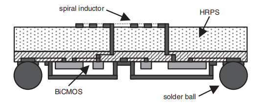
A solution to these problems can come from an integration of the passive components over or under the active circuitry . This can be accomplished by using a spacer substrate, having low RF loss, a high permittivity, and good thermal conductivity. This spacer substrate is inserted in between the active chip and the passive components and can be applied in wafer-level packaging (WLP), as shown in Fig. 1.
Glass substrates that have been proposed for passive component integration could be considered for this purpose. Glass, even though used in WLP for some applications , has, however, a low dielectric constant and a poor thermal conductivity. Silicon is superior in both aspects and can provide low loss fifigures if high-resistivity silicon (HRS; 1–10 kO cm) is used . Single-crystalline flfloat-zone HRS wafers, however, are expensive and prone to surface-channel effects unless an additional surface-passivation step is added .
In this Letter, high-resistivity polycrystalline silicon (HRPS), which can be adopted from the early phase of flfloat-zone wafer preparation (wafers from high-resistivity polysilicon rods), is proposed as a novel cost-effective alternative to glass and HRS RF substrates.

Fig1
Results and discussion: The dielectric constant (Fig. 2a) and the total loss (Fig. 2b) were obtained from S-parameter measurements up to 10 GHz. Good agreements of the measured data and simulations in ADS-Momentum were obtained for all CPW structures and substrates shown in Fig. 2. In comparison to the glass substrates, i.e. Pyrex 7740 (a ¼ 0.7 dB=cm), Hoya SD-2 (a ¼ 0.37 dB=cm) and Schott AF45 (a ¼ 0.38 dB=cm), a comparably low loss fifigure was measured for HRPS with (a ¼ 0.44 dB=cm) and without (a ¼ 0.89 dB=cm) an insulation oxide layer at 6 GHz. Given this result, HRPS offers several advantages in comparison to glass, such as the higher and nearly frequency independent dielectric constant (11.7 against 4.8–6.2; Fig. 2a) allowing for a 30–35% more compact component integration, the >10-times higher thermal conductivity, the perfect matching of the thermal expansion coeffificient to that of the integrated circuit (IC) wafer, and the full compatibility with silicon processing. The fact that a low loss tangent could be demonstrated for HRPS without an insulation oxide layer is signifificant, because metal vias through the HRPS substrate can therefore be built without any complicated dielectric liner formation (Fig. 1). In comparison to HRS, no additional surface passivation steps are required for HRPS, as seen from the 30 GHz S-parameter data in Fig. 3; that is, because the material has an inherently high defect density (Fig. 4), suppressing any surface channel formation similarly to the surface amorphisation to passivate the HRS . Moreover, CPW T-resonators having quality factors Q¼ f0=f3-dB > 18 demonstrated the low loss of HRPS, while eliminating any de-embedding error. High Qs of 7.5 and 11 were measured for the 34 nH spiral inductor with and without an insulating oxide layer, respectively, thus providing further evidence of the excellent RF quality of the HRPS substrate.
Coplanar waveguides (CPWs), which are particularly sensitive to surface effects, were used as test structures to evaluate the RF losses of glass, HRS and HRPS substrates. A CPW T-resonator and a large (34 nH) spiral inductor were included with that test site as well. A 2 μm-thick aluminium (Al) metallisation was used in all cases. CPWs on the HRPS were formed with and without a 1 μm-thick PECVD oxide isolation layer. The HRS wafers had an oxide isolation with or without a surface passivation . Three types of glass substrates were included with our evaluation, i.e. Pyrex 7740, Hoya SD-2 and Schott AF45. The CPW test structures were designed with different signal-ground spacings in order to achieve impedances close to 50 O in all cases and to allow for meaningful comparisons. CPW length of 0.5, 1, 3 and 5 mm were used.
HRPS has been presented and demonstrated as a novel RF substrate for wafer-level packaging and passive component integration in general. The material provides very low RF loss compared to that of glass, a high dielectric constant to allow for compact passive component integration, a high thermal conductivity, and a perfect match of the thermal expansion coeffificient to that of the IC wafer. Finally, HRPS is fully compatible with silicon processing and is a low-cost alternative to HRS wafers.
下一篇: NiW 合金电镀填充 TSV