After Damascus revolution, the metal copper as conductive material and CMP (chemical mechanical process) technique replacing an old process in the industry, have led to an industrial transformation. To meet the requirement of state-of-the-art electronic products, more and more different materials and devices must be stacked together to reduce the volume of IC chips and signal transmission delay. Electrodeposition plays an important role in metallization development, especially copper electrodeposition, which is a critical technology and generally used in 3D (Three-Dimensional) chip packaging.
For the future technological trends of the 3D packaging, TSH (Through Silicon Hole) and TSV (Through Silicon via) connection play a key role in the manufacturing process, where copper process dominates the final reliability. However, the packaging materials with different CTEs (Cu: 17.5 ppm; Si: 2.5 ppm) will induce large stresses at the interfaces, resulting in cracks and extrusion defects between dielectric layer and silicon substrate.
To reduce the thermo-mechanical stress and effectively enhance durability of silicon wafer we use tungsten as a filling material, which has similar physical characteristic (W CTE: 4.5ppm) to silicon to enhance the durability of the silicon wafer.

Fig1
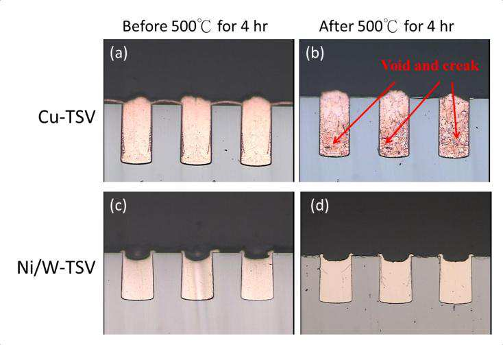
Figure 1. Thermal reliability test of Cu-TSV and Ni/W-TSV. A lot of small voids and creak were observed in the Cu-TSV after the thermal annealing treatment at 500℃ for 4 hr. The issue did not occur in the case of Ni/W-TSV. The structure of the Ni/W-TSV was still intact after the thermal annealing at 500℃ for 4 hr.
The traditional process for making TSV is a dry process. It includes many steps, from the via formation to the copper eletrodeposition of copper in via. We replace the copper by Ni-W alloys and reduce the TSV process without Cu seed layer deposition. The process promotion can reduce the cost and solve the issue of CTE mismatch.
According to an empirical equation[3] of Ni-W CTEaverage, we can predict the CTE value by calculating tungsten content in the alloy. Figure 1 shows the results of thermal reliability test. A lot of small voids and creak were observed in the Cu-TSV after a thermal annealing treatment at 500℃ for 4 hr. In addition, copper protrusion on the TSV was also obvious after the thermal annealing. However, these issues did not occur in the case of Cu-free TSV (Ni/W-TSV). The structure of the Ni/W-TSV was still intact after the thermal annealing at 500℃ for 4 hr, indicating that Ni-W alloy is very stable because of its low CTE.
上一篇: 高阻多晶硅作为晶圆级封装中的射频基板
下一篇: 多孔硅的导热率、光导率和电导率的变化