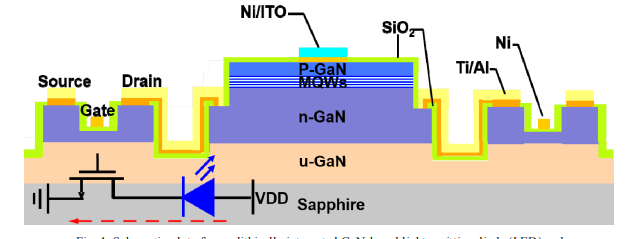
In this study, we report a novel monolithically integrated GaNbased light-emitting diode (LED) with metal-oxide-semiconductor fieldeffect transistor (MOSFET). Without additionally introducing complicated epitaxial structures for transistors, the MOSFET is directly fabricated on the exposed n-type GaN layer of the LED after dry etching, and serially connected to the LED through standard semiconductor-manufacturing technologies. Such monolithically integrated LED/MOSFET device is able to circumvent undesirable issues that might be faced by other kinds of integration schemes by growing a transistor on an LED or vice versa. For the performances of resulting device, our monolithically integrated LED/MOSFET device exhibits good characteristics in the modulation of gate voltage and good capability of driving injected current, which are essential for the important applications such as smart lighting, interconnection, and optical communication.
Figure 1(a) shows a schematic configuration of monolithic integration of GaN-based LED and MOSFET. An LED structure was grown onto 2-inch sapphire substrates using a lowpressure metal-organic chemical vapor deposition (Aixtron 2600G) system. The LED layerstructure comprised of a 30-nm-thick GaN nucleation layer grown at 520°C, a 2-μm-thick undoped GaN layer grown at 1050°C, 2-μm-thick Si-doped n-type (n = 5 × 1018 cm−3 ) GaN cladding layer grown at 1050°C, an unintentionally doped active region of five periods InGaN/GaN MQWs grown at 700 °C with emitting wavelength of λ = 485 nm, and a 200- nm-thick Mg-doped p-type (p = 3 × 1017 cm−3 ) GaN layer grown at 800°C. The low growth temperature of p-type GaN layer is to roughen its surface for enhanced light extraction efficiency of the LED. The LED structure was then selectively removed by dry etching (inductively coupled plasma, ICP) with Ar/Cl2 mixed gases to expose the n-type GaN layer for the subsequent fabrication of MOSFET. A 2-μm-deep trench down to the undoped GaN layer was created to isolate the LED and MOSFET mesa regions by an additional ICP process. A 500-nm-thick SiO2 passivation layer was then deposited on the sidewalls of LED and MOSFET mesas by plasma-enhanced chemical vapor deposition (PECVD). Next, the remaining of n-type GaN layer on top of the MOSFET mesa was patterned by standard photolithography and ICP dry etching that gives a film of 150 nm for the current channel. After that, a 200-nm-thick SiO2 layer was deposited as a gate dielectric by using PECVD again at an operating temperature of 300°C. Ti/Al was deposited by e-beam evaporation and annealed by rapid thermal annealing (RTA) at 600°C for 30sec in N2 ambient for source/drain contact metals of the MOSFET and cathode of the LED. ITO/Ni was deposited by the RF magnetron sputtering, patterned by lift-off process, and annealed at 450°C for 2 minutes in O2 ambient to form p-type ohmic contacts for the LED. Finally, Ni was deposited and patterned as the gate electrode of the MOSFET.

Fig1
We first examine the DC characteristics of the fabricated device. Figure 3(a) shows output ID-VD measurements of the monolithically integrated LED/MOSFET device with the applied gate voltage (VGS) ranging from VGS = −1.5V to 2V in 0.5V interval. The maximum output current of IDS = 1050 mA/mm is achieved under VGS = 2V, and the specific on-resistance (Ron) is estimated to be Ron = 105Ω. The output characteristic of the MOSFET is comparable to that of previously reported monolithically integrated structures based on GaN-based HEMT devices. Figure 3(b) shows the transfer characteristics of the MOSFET for the applied source-to-drain voltage of VDS = 2V, 4V, and 6V. The MOSFET exhibits a peak transconductance of Gm = 368 mS/mm at VDS = 6V, and achieves an OFF-state drain leakage current as low as Ioff = 2.47 × 10⁻⁵ mA/mm at VDS = 2V. The DC characteristic shown in Fig. 3 suggests that the performance of the MOSFET is acceptable, and hence can be monolithically integrated with the LED device. It shall be addressed again that the MOSFET was fabricated on the exposed n-GaN layer after dry etching, and no additional growth layers of HEMT was employed in this study. Thus such device structure of monolithically integrated LED with MOSFET is more direct and also feasible without introducing other undesirable issues as previously reported in the literatures.
Next, we are able to test the performance of the monolithically integrated LED/MOSFET device. Figure 5(a) shows LED’s current (same as the source-to-drain current, IDS) and light output power (LOP) versus supply voltage across the entire device (VDD) for different gate voltages ranging from VGS = −1V to 1V in 0.5V interval. Due to the serially connected configuration between the LED and MOSFET devices (as the equivalent electrical circuit plotted in the inset of Fig. 1), IDS is therefore restricted by the LED before its turn-on, and becomes saturated and dominated by the channel current of MOSFET while further increasing VDD. Obviously, by a simple control of the MOSFET’s VGS, we are able to modulate the injected current and light output power of the LED with good linearity. As shown in the inset of Fig. 5(a), we demonstrate a LED light-switch (red line) with an ON/OFF frequency of 10kHz by directly modulating the VGS of the MOSFET (black line) and the IDS injected into the fabricated device (blue line). Similarly, Fig. 5(b) shows IDS and LOP versus VGS of the monolithically integrated LED/MOSFET device for the supply voltage of VDD = 7V and VDD = 15V. Again, the saturation of IDS and LOP observed on the operating condition of VDD = 7V is mainly due to the limited current within the MOSFET channel. By increasing the supply voltage to a larger value of VDD = 15V, both IDS and LOP increases linearly with the increasing of VGS. Observations in Fig. 5 indicates that our monolithically integrated LED/MOSFET device exhibits good characteristics of gate controllability and current driving capability, which are essential for various applications such as smart lighting, interconnection, and optical communication.