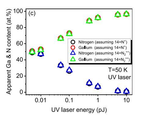
With scaling of semiconductor devices showing no signs of abating and three-dimensional structures now being developed, new metrologies to meet these demands are being sought. Atom probe tomography offers the potential to meet these challenges, and here, the authors present an in-depth study focused on fifinding useable conditions for accurate stoichiometric analysis of GaN and AlGaN. By varying the laser energy/power, changes in the average tip fifield were induced, and the resulting impact on the measured stoichiometry was investigated. A strong variation in the GaN stoichiometry as a function of the average tip fifield was found, although a range of conditions that enable accurate stoichiometry were determined. Moreover, the stoichiometric variation as a function of tip fifield was highly reproducible across instruments and laser wavelengths. However, for AlGaN, the N concentration was always underestimated. To try and establish the underlying cause of the N underestimation, potential loss mechanisms which include N2 sublimation, N2 neutral generation from molecular ion dissociation, and differences in the fifield of evaporation between the matrix elements and multihits were considered and are reported herein.
With the continuous scaling and simultaneous move toward complex three-dimensional (3D) semiconductor device architectures to meet future device technology needs, a corresponding shift in metrology is required. Additionally, metrology is increasingly being required to guide novel material, device, and technology development and as such faces multiple challenges related to spatial resolution, analyzable volume, speciation, and quantifification.1 Atom probe tomography (APT) has emerged as one of the few techniques capable of dealing with the nanometric dimensions of novel devices and offers the potential to meet, in general, the above-mentioned metrology challenges. This is because APT has a theoretical lateral (0.3–0.5 nm) and depth (0.1–0.3 nm) resolution capability. However, APT is still a relatively new technique for semiconductor material analysis because its applicability within this fifield was only realized with the more recent advent of laser assisted APT.2 As such, there are still many underlying aspects of the technique requiring investigation and understanding if it is to establish itself as a routine and reliable metrology technique for future generation semiconductor technologies.
A bulk GaN sample alongg with a range of AlGal N(x= 0.08, 0.44, and 0.75) samples was used for this study. Allthe samples were grown by metal organic chemical vapordeposition. The atom probe (AP) analysis tips were preparedby the conventional focused ion beam (FlB) lift out approach using an FEI NOVA 600 or FEI Helios 450 FIB/SEM. Thefinal tip diameter for all the samples was in the range of50-100 nm, while a 2 kV (~10pA) Ga beam clean prior toloading into the atom probe was adopted. The AP measure-ments were taken on either a Cameca LEAP 5000XR AP or aCameca LA-WATAP In the case of the LEAP 5000XR AP, aUV laser (A = 355nm) was used, while for the LA-WATAP agreen laser (A= 515 nm) was utilized. The laser energy(power) used for this work ranged between 0.005 to 15 pl onthe LEAP and 100 to 10000 uW for the LA-WATAP, with 400 000-500000 atoms per dataset collected. Analysis was performed at a base temperature of either 25 or 50k and aconstant detection rate of 0.5% (=0.005 atoms/pulse) for theLEAP and 0.005-0.008 atoms/pulse for the LA-WATAP used.The collected data were subsequently analyzed using either theIVAs 3.6.12 software or TaP3D, both provided by Cameca.

Fig1
Again, we identify the onset of DC evaporation processes by recording the mass background counts versus fifield (Fig. 3). Different from GaN, the AlGaN cases allow much higher fifields to be used, leading to increased backgrounds indicative of an increased DC evaporation when laser power is decreased. The very small rise in DC evaporation between Gaþþ/Gaþ ¼ 0.001 and 2 is thought to be from Ga and Al [FOE (Ga) ~15 V/nm, FOE (Al) ~19 V/nm], while the large increase at higher tip fifields, i.e., Gaþþ/Gaþ 2, is believed to be from the onset of N DC evaporation which will be discussed in more detail later in this paper.
Unlike GaN, the behavior when varying the measurement conditions was found to be different and conditions for stoichiometric analysis were never observed. To try and understand the underlying reason for this, we have studied how the combined Al þ Ga and N concentrations, as well as just those of the group III materials, vary as a function of the average tip fifield (Gaþþ/Gaþ ratio). An attempt to relate these fifindings to some of the potential loss mechanisms such as N sublimation, neutrals generated from molecular ion dissociation, preferential evaporation due to differences in the elements FOE and multihits has been made and are presented below.
下一篇: 湿基材表面清洁