Ultraviolet (UV) photodetectors have drawn extensive attention owing to their applications in industrial, environmental and even biological fields. Compared to UV-enhanced Si photodetectors, a new generation of wide bandgap semiconductors, such as (Al, In) GaN, diamond, and SiC, have the advantages of high responsivity, high thermal stability, robust radiation hardness and high response speed. On the other hand, one-dimensional (1D) nanostructure semiconductors with a wide bandgap, such as β-Ga2O3, GaN, ZnO, or other metal-oxide nanostructures, also show their potential for high-efficiency UV photodetection. In some cases such as flame detection, high-temperature thermally stable detectors with high performance are required. This article provides a comprehensive review on the state-of-the-art research activities in the UV photodetection field, including not only semiconductor thin films, but also 1D nanostructured materials, which are attracting more and more attention in the detection field. A special focus is given on the thermal stability of the developed devices, which is one of the key characteristics for the real applications.
The well-established UV-enhanced Si technology has some limitations in the UV detection. Since the bandgap energy of Si is 1.1 eV, costly high pass optical filters and phosphors are needed to stop low energy photons. Therefore, the device performance is degraded with temperature, as evidenced by lower efficiency and increasing dark currents. The development of wide-bandgap-semiconductor UV photodetectors has now emerged, such as GaN-based system, diamond, or SiC-based system, which do not need the insertion of filters, showing their potential for high-temperature applications. Recently, we found that the detectors can work at the temperature up to 523 K by using calcium fluoride (CaF2) as the insulation layer in a InGaN-based metal-insulator-semiconductor (MIS) Schottky-type photodiodes. On the other hand, one-dimensional (1D) nanostructured UV detectors are attracting more and more attention owing to the improved sensitivity to light due to their large surface-to-volume ratio and Debye length comparable to their small size. An enhanced photosensitivity has been observed in 1D nanostructured UV detectors, such as ZnO nanowires, Ga2O3 nanowires and nanobelts, GaN nanowires, or other metal-oxide nanostructures. However, as a result of the surface dominated photocurrent transport, the high-temperature UV detection based on the nanostructured semiconductors are facing predicaments. To resolve this bottleneck, bulk-dominated photocurrent dynamics are preferred.
Due to the interesting applications, including early missile threat detection and interception, chemical and biological threat detection, UV flame monitoring, UV environmental monitoring, etc., there have been tremendous developments in the field of solar-blind photodetectors with a cut-off response lower than 280 nm using AlGaN since 1999.

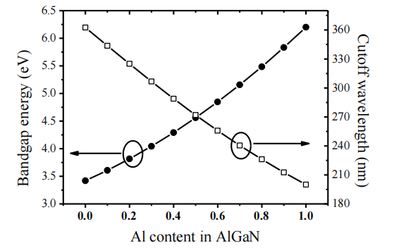
Fig1
Figure 1 shows the relationship of bandgap energy (cutoff wavelength) of AlxGa1-xN semiconductor with Al mole fraction. As can be seen, to realize solar-blind detection, the Al composition in AlxGa1-xN should be higher than 40%. High-quality AlGaN films are the key element in obtaining high-performance photodetectors. Compared to GaN, the growth of AlGaN especially with a high Al amount has proved to be significantly difficult, which lies in the lower migration of Al atoms than that of Ga atoms, and strong parasitic reactions. Therefore, the layer-by-layer growth with the atomic steps on the surface for the films is difficult to achieve compared with the well-developed GaN template. As a result, high-density defects, such as dislocations, grain boundaries, or stacking faults, are much easier to generate.
Previously, AlGaN films were usually deposited on GaN templates to fabricate UV devices. However, as a result of the tensile strain from the smaller in-plane lattice constant of AlN compared to that of GaN, cracks were generated when the thickness of the AlGaN film was higher than its critical thickness. On the other hand, to avoid the optical absorption from contacts, back-illuminated configurations are needed for the Schottky or p-i-n type photodetectors. Nevertheless, most of the UV light was absorbed by the narrow-bandgap GaN template. AlGaN films grown on sapphire consist of many fine mosaic blocks, which also result in the cracks due to the coalescence of these blocks. The cracks result in a high dark current of µA or mA, a low rejection ratio, and restrict the performance of the UV devices. The highest Al composition without cracks obtained on GaN template is ~30% by using the interlayer technique. The best performance of the AlGaN photodetectors on GaN template used the Schottky structure, and showed a dark current of 9 nA at −5 V, cutoff wavelength of 310 nm, and UV/visible discrimination ratio of 104 .
上一篇: 半导体中电流的亚周期光学控制
下一篇: 消除氧化过程中产生的多晶硅孔缺陷