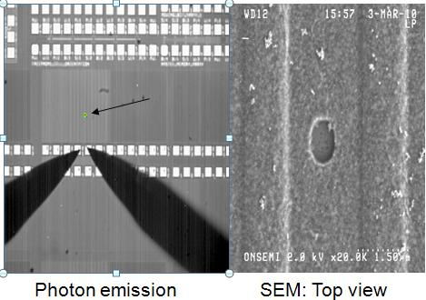
Gate Oxide failure analysis during technology qualification led to discovery of the polysilicon hole defects in large (>200Kμm² ) PMOS capacitors. In-line KLA inspections confirmed that polysilicon holes were formed during the salicide block process module. It is hypothesized that a three way interaction between the P+ source/drain implanted boron, heat added during salicide block mask deposition, and NH4+ in the BOE causes the polysilicon hole. By replacing the BOE (Buffered Oxide Etchant) with a 100:1 HF solution, the creation of polysilicon holes was eliminated as confirmed by KLA and VBD testing.
Gate oxide failures are one of the major contributors to the reliability and yield loss of semiconductor devices. While most gate oxide issues are created within the gate oxide module, this paper will demonstrate that post gate processing can contribute to gate oxide defects. Specifically, defects formed during the salicide block module on polysilicon; a module that serves as a hard mask for selective salicide formation.
An in depth investigation revealed that failing gate oxide test results were due to polysilicon holes that formed in the salicide block module, during the pre-metal-deposition cleans. Subsequent silicide formation in the polysilicon hole caused electrical shorts. While not directly related to inherent oxide quality, the failures appeared as extrinsic gate oxide defectivity.
As part of a high voltage 0.35um technology qualification, gate oxide integrity tests including TDDB and VBD were performed. TDDB and VBD tests showed that PMOS GOI capacitors exhibited high failure rates on PCSQ1 (large square active area), PCPE1 (poly edge) and PCBB1 (Birds Beak) structures, while all complimentary NMOS structures were relatively defect free. Data analysis indicated that the failures were Type-A extrinsic defects in nature. Excluding these failures otherwise indicated that the intrinsic lifetime for the gate oxide met the 10 year requirements. Table 1 outlines the test structure types, its dimensions, and it failure rate.

Fig1
Stepwise scan recipes were developed to determine where in the salicide block processing module that the defect type was first formed. For these inline scans, a relative visual Defect Density (D0) was determine through review of the defects found with KLA scans. D0 is defined as number defects per square centimeter of area scanned. Through the in-line scans, the polysilicon defect was determined to be first detected after pre-metal clean. This clean is used to remove any native oxide prior to Ti deposition and can be considered as primary process step in the creation of polysilicon hole defects. With this discovery, additional experiments were performed to identify contributing factors to the defect formation and to understand the mechanism of polysilicon hole formation.
A short-loop flow was created based on salicide block module utilizing patterned implanted wafers. With the shortloop flow wafers, many experiments were designed to find the root cause for the defect of interest. Below are summaries of the important experiments that lead to determining a root cause for the polysilicon holes defects. All experiment results are based on visual defect counts.
One theory to the defect formation was that the P+ implant is physically damaging the poly-silicon and allowing the pre-metal clean to remove the damaged polysilicon. An experiment designed to test this theory used B, BF2, and Ar as implant species with same dose and energy condition as the standard P+ source/drain implant used by the technology. The inert Argon gas was chosen to only study the physical damage effect of an implant on the polysilicon.
上一篇: 半导体紫外光电探测器的研究综述
下一篇: 光刻模块标准步骤