A simple and low-cost process was devised to elim-inate etch damage resulting from oxide etching on the seed-holesurface prior to selective epitaxial growth (SEG) of silicon. Theprocess consists of a low power CaFs RIE step which wasperformed right after the oxide etch step in the same etch reactor.The use of this step excluded the need of a conventional sacrificialoxide to remove damaged silicon regions and residual polymers.The N/P diodes resulting from N-type SEG grown on P-typesubstrate were used to evaluate the quality of the silicon surfaceprior to SEG.
In this letter, we present a process flow which eliminatesthe need of the sacrificial oxidation. After the seed-hole oxidewas etched in a CHFs/C2Fs RIE, a short, low power CzFsetch was performed. These wafers were compared with twoother process flows: 1) wafers in which the sced-hole waswet-etched, 2) wafers where oxide was etched in CHF3/C2FgRIE, and 3) wafers where a reoxidation step was performedafter the dry-etch. N-type SEG silicon was grown in P-type(100) substrates in all wafers and the resulting diode formed at the substrate/SEG interface was used to evaluate the quality ofthe interface and hence the quality of the silicon surface priorto SEG. The diodes formed on wafers with the low powerC2Fs etch and no sacrificial oxidation exhibited ideality factorswhich were the same as the diodes resulting from the wet-etched seedhole and the reoxidized seed-hole diodes. The newprocess flow provides a very simple and cost-effective way toeliminate RIE damage prior to SEG growth because the drylow power CzFs etch can be done in the same etch reactorin which the seed-hole oxide etch is performed. In addition,the reoxidation step is eliminated, hence, reducing the numberof process steps.
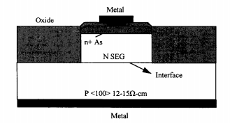
All wafers were then cleaned in a megasonic clcaner inH2O2:NH,OH solution. The wafers were then placed in aApplied Materials 7800 barrel reactor, A two minute H2 bakeand a 30 second HCl etch, both at 980°C, were used priorto the growth, SEG was then grown from the silicon seed-holes at 980°C, 40 torr at a growth rate of 0.17 pm/min toresuit in i um of growth, The SEG was arsenic doped at aconcentration of 7x 1015 cm-3, After the SEG, arsenic wasimplanted in the n-type silicon at 60 keV with a dose of5x 1015 cm-3. LTO was deposited and densified at 1050°Cfor 15 minutes which also activated the implant. Contacts wereopened and the wafers were metalized. The cross-section ofthe fabricated diodes is shown in Fig. 1.
The purpose of this letter was to report the results of asimple and manufacturable process to produce high qualitysilicon surface prior to selective epitaxial growth. A low powerC2Fs etch was used after the oxide etch in the same reactorto remove residual polymers and RIE damage. N-type SEGwas grown on P-type substrate to form diodes and evaluatethe interface quality and hence the surface preparation prior toSEG. It was shown that the diodes with the in-sifu C2Fs etchresulted in excellent surface quality, thus eliminating the needfor the conventional sacrificial oxidation step.

Fig1
The purpose of this letter was to report the results of asimple and manufacturable process to produce high qualitysilicon surface prior to selective epitaxial growth. A low powerC2Fs etch was used after the oxide etch in the same reactorto remove residual polymers and RIE damage. N-type SEGwas grown on P-type substrate to form diodes and evaluatethe interface quality and hence the surface preparation prior toSEG. It was shown that the diodes with the in-situ C2Fs etchresulted in excellent surface quality, thus eliminating the needfor the conventional sacrificial oxidalion step.
上一篇: 远程检测晶圆夹持装置上的电镀
下一篇: 单晶圆清洗