Metal-assisted chemical etching (MACE) is a simple, low-cost and versatile method of fabricating various silicon nanostructures. Due to the etching anisotropy of monocrystalline silicon, i.e. its different crystal orientation has different number of silicon back bonds needed to be broken in the etching process, the obtained silicon nanostructures are morphology variable. It has been demonstrated that, by choosing the species or morphologies of catalyst, adjusting the etchant composition or concentration, changing the doping species and level of the silicon substrate, or introducing extra physical fifields, MACE method can be used to prepare various desired silicon nanostructures. This review summarizes the most recent contributions in the fabrication of designable monocrystalline silicon nanostructure by MACE. In order to provide a relatively complete comprehension of the MACE, the fundamental principle and basic manipulation process of a conventional MACE, as well as the main inflfluence factors on the etching effects are given; and the common applications of MACE in silicon etching are brieflfly reviewed. This article also presents some new developed improved MACE technologies and their potential applications in the extended fifield.
The approaches for the fabrication of silicon nanostructures can be brieflfly classifified into two schemes, the bottom-up and topdown ones. For the bottom-up scheme, the most representative method is the ‘vapour–liquid–solid’ (VLS) growth. In this method, catalytic liquid alloy phase is introduced as the seed, which can catalyze the dissociation of the silicon gas with the freed silicon atoms, rapidly adsorbing them to supersaturating levels; then, the silicon atoms dissolve out and arrange to crystalline silicon nanostructures. As the VLS growth is a quasi-stationary thermodynamics process, it can be used to fabricate relatively high-quality silicon nanowires (SiNWs). The top-down scheme can be further separated into dry and wet etching approaches. The most commonly used dry etching approach is the inductively coupled plasma (ICP) etching, which utilizes plasma reaction gas to etch the silicon substrate with mask and can provide fairly good etch rates and anisotropy. And the typical wet etching approach is the metal-assisted chemical etching (MACE) method, in which the silicon substrate immersed in the etchant is etched into various nanostructures with the assistance of metal catalyst.
Cost-efficiency and equipment requirement are two factorsmust be considered, for the widespread applications of everyapproaches mentioned above. The VLS and ICp methods bothrequire large equipment, so they cannot be afforded by mostlaboratories. Additionally, the processes of them are high-cost.since they both need high purity gases, vacuum technology andhigh temperature (or high power magnetic coil); moreover, theyalso have a certain dangerous nature because they both requireinflammable dangerous gases. Due to these negative factors, only afew of research teams still use the VLS and ICp methods infabrication silicon nanostructures, Conversely,the MACE method isthriving and developing day by day, since it only requires verysimple equipment (a beaker), and the silicon nanostructuresprepared by this method are designable by adjusting the etchingprocess.
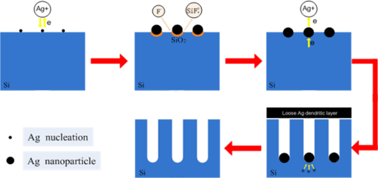
MACE is a very simple technique in fabricating silicon nanostructures. The basic manipulation of it even only requires a beaker. The manipulation process can be brieflfly separated into three steps: Firstly, cleaning the silicon substrate and confifiguring the etching solution for later use;then, immersing the silicon substrate into the etching solution and maintaining a period of time; fifinally, taking the silicon substrate out and rinsing it with deionized water. Such a simple technique can be afforded in any laboratory, and meanwhile can be used to prepare many interesting silicon nanostructures with low cost.

Fig1
From being developed, the most common applications of MACE are to fabricate various vertical, large aspect ratio SiNWs and silicon Si nanoholes (SiNHs). Of them, SiNW has been widely used for light-trapping in photovoltaic devices and been regarded as one of the most attractive building blocks for many future optical and optoelectronic devices; SiNH can be also effectively used to enhance light harvesting in solar cells, like the famous black silicon solar cells . There are abundant reports that have been published on this issue. Here, we just brieflfly reviewed some representative literature and some works of our group, so that the reader can have an intuitive understanding on the application of MACE but we did not pursue summarizing all of the articles related.