Yeld analysis is an activity common to all companies manufacturing semiconductor devices on an industrial scale and consists in identifying problems relating to thcproduction cycle by analyzing the number and distribution of non-functioning chipson the wafer. This is an extremely expensive activity from the point of view of human resources employed because it requires the visual analysis of thousands of mapsgraphical representations of the distribution of non-functioning chips) on silicon wafersproduced and analyzing a huge amount of (not only) electrical related data. On theother hand, yeld (percentage of chips running on a wafer) analysis is absolutely essen.tial, because it is linked directly to the marketing and the potential profit margin ofproduced devices.
Schematically, this activity can lead to a problem of recognition of models (knownissues, typically dealt with supervised neural networks) in a high noise environment,. orhow to bind the data to different wafers based on models that are not known a priorisearch for unknown problems, or clustering, dealt with appropriate algorithms and/orwith unsupervised neural networks).
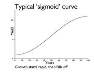
The production of integrated circuits usually includes a large number of very complexprocesses 1 a investment on the order of billions of dollars. For this reason the yieldnas always had a fundamental role in maintaining the level of competitiveness: becomingalmost co-own production costs, the amount of profits is determined solely by the numberof good chips manufactured wafer (resa). This makes the attempt to improve it (yieldenhancement) activity continues in any industry. According to 2 , relating to a particulardevice can be rappresetata graphically as a function of its life cycle. In fact, dependingon how they consolidated design, processes and technologies, elements which negatively onfinal rendering can be different (see Fig. 1).

Fig1
The life of an electronic device is divided primarily into four phases. The first is theexperimental phase, in which several experiments are carried out in line in order to establishcertain operating parameters. The main cause of yield loss at this stage is represented bydevices operating out of specifcation. After this phase occurs the formation of systematicdefects, born from the particular sensitivity of yeld to certain specific aspects of the designor manufacturing processes. Some circuits can fail for electrical effects or interactions evenif there are no physical defects directly involved: is this the case, for example, of cross-talkbetween metal connections.
Other defects can arise from the systematic difference, in terms of layout, between theproject and its realization. The frequency with which you have unexpected defects as opencircuits, short circuits, incorrect values of resistivity, defects due to imperfect alignment othe various layers. errors due to the networks of photolithography, wrong critical dimensionsand so on increases as one approaches the natural tolerance limits of the particular processtool inwolwed.
In this scenario, you add the so-called ercursions, i.e. the sudden and intermittent yieldlosses due to malfunctions of processing machinery or changes in process environmentsExcursions can cause an unexpected increase in the yield loss on some lots or wafers. oeven only on certain areas of the wafers themselves. The search and identification of thecauses of these defects requires a large amount of data and a not simple analysis, but itplays a significant role in raising the semiconductor manufacturing yield.
The last section opens with a description and some examples of application of a clustering algorithm used to identify defective chip patterns of wafers, and concludes withguidelines for the development of appropriate supervised neural networks suited to therecognition of known yeld problems, to be used to match defective wafers towards thepatterns highlighted by the previous clustering.