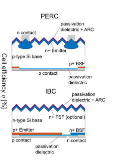
Silicon wafer solar cells continue to be the leading photovoltaic technology, and in many places are now providing a substantial portion of electricity generation. Further adoption of this technology will require processing that minimises losses in device performance. A fundamental mechanism for effificiency loss is the recombination of photo-generated charge carriers at the unavoidable cell surfaces. Dielectric coatings have been shown to largely prevent these losses through a combination of different passivation mechanisms. This review aims to provide an overview of the dielectric passivation coatings developed in the past two decades using a standardised methodology to characterise the metrics of surface recombination across all techniques and materials. The effificacy of a large set of materials and methods has been evaluated using such metrics and a discussion on the current state and prospects for further surface passivation improvements is provided.
Silicon wafer solar cells are the fastest growing and most successful photovoltaic technology to date. The past decade witnessed remarkable technical and economical milestones: (i) record breaking single junction cells with power conversion effificiencies exceeding 26% ; (ii) multicrystalline silicon cells, which account for over 60% of the PV market, that now have effificiencies exceeding 20%; (iii) a continued average annual growth in the PV market of more than 40% over the past decade ; (iv) a vast reduction in module production costs bringing the $/Wp of solar energy below grid parity in many places around the world; and (v) energy payback times now below 1 year.
To keep the growth and deployment of this technology, industry and academics continue to research ways to increase cell effificiency and/or reduce its production cost. Out of these two approaches, improved effificiency has the greatest scope to impact the overall cost of solar electricity since it affects the entire value chain. The production and processing of silicon has largely improved in the past decades. This has reduced the negative effects of bulk impurities in cell performance. Cost reduction has also driven cells to become increasingly thinner. These successes meant that the efforts to improve further device performance have shifted towards surface physical phenomena, mainly the passivation of surfaces and interfaces. Surface passivation helps to prevent unwanted recombination of photogenerated electron–hole pairs. As such, it is a key requirement to achieve high conversion effificiencies. In fact, a large portion of the improvement achieved in record-breaking silicon cells has been possible due to outstanding surface passivation. This is demonstrated, for example, by the use of amorphous silicon passivation in Kaneka’s 26.6% and Panasonic’s 25.6% cells, or aluminium oxide passivation of p-type silicon combined with thin oxide electron selective contacts in Fraunhofer ISE 25.7% TOPCon cell.
Here, the widely adopted An observation is made with regards to nomenclature. fifield-effect passivation terminology has been used, but it is important to note that, in the absence of external stimulation, the electric fifield and associated charge distribution established in the near surface region is in equilibrium. Therefore the electric fifield cannot repel excess minority carriers away from the surface. This electric fifield, however, modififies the surface carrier concentration, which in regimes of heavy accumulation and inversion, leads to a reduction in recombination rates upon carrier excitation. Thus, strictly speaking, the reduction in surface recombination is due to the spatial change in carrier concentration near the surface, which in turn is due to the electric fifield. This distinction has recently been pointed out by Cuevas. However, the term ‘fifield-effect passivation’ has been retained for the present work since it is in wide use throughout the literature and it is clear that an electric fifield is created in the silicon near surface region by doping or by dielectric charge, as originally pointed in the early 1950s by Shockley and Pearson in the context of the fifield-effect transistor.

Fig1
As stated in previous section, higher recombination is typically observed at a textured surface. The front of a solar cell will normally be textured, and the passivation may not be as good as for flflat surface. It was noted that, despite the very effective passivation methods review in the next section, the recombination at a textured surface can be over one order of magnitude higher than in a flflat surface. This will substantially increase J0e.
As the solar cell industry has progressed, it has become a requirement to produce large volumes of cells cost effectively. This has motivated the production of largethroughput dynamic PECVD reactors, much different than the static ones in laboratory facilities. A very complete investigation on PECVD inline production of SiOx dielectrics has been conducted in recent years by Duttagupta. Along with other reports, it was demonstrated that only relatively poor passivation is achieved when using such PECVD SiOx fifilms (Seff > 100 cm s-1 in moderately doped silicon) even after temperature treatments and extrinsic H passivation via FGA. To address this issue a second capping layer is commonly deposited on top of an interfacial SiOx to produce a bilayer stack, typically using silicon nitride (SiNx) or aluminium oxide (AlOx). These multi-layered fifilms will be described later in this paper.
It is evident that extensive work has resulted in extremely effective plasma nitride fifilms. To complement these advances, high throughput industrial tools have been developed, where dynamic deposition allows inline manufacture of solar cells. Some studies investigated these industrial techniques yet with limited success. The work of Duttagupta covers the most substantial progress in this area. He found Seff under 1.82 and 2.46 cm s-1 in 1 Vcm n- and p-type Si using nitride fifilms deposited in industrial scale inline PECVD reactors. In similar studies Duttagupta investigated the passivation mechanisms of these fifilms and found that the effectiveness of passivation was mainly due to the fifieldeffect repulsion of carriers from an intrinsic fifixed charge concentration of 3–5 x10¹² q/cm2 . A smaller effect due to the chemical component was suggested.