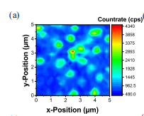
We investigate native nitrogen (NV) and silicon vacancy (SiV) color centers in commercially available, heteroepitaxial, wafer-sized, mm thick, single-crystal diamond. We observe single, native NV centers with a density of roughly 1 NV per µm3 and moderate coherence time (T2 = 5 µs) embedded in an ensemble of SiV centers. Low-temperature spectroscopy of the SiV zero phonon line fifine structure witnesses high crystalline quality of the diamond especially close to the growth surface, consistent with a reduced dislocation density. Using ion implantation and plasma etching, we verify the possibility to fabricate nanostructures with shallow color centers rendering our diamond material promising for fabrication of nanoscale sensing devices. As this diamond is available in wafer-sizes up to 100 mm it offffers the opportunity to up-scale diamond-based device fabrication.
Diamond nanostructures are of signifificant importance for various applications in science and industry including nanomechanical devices, photonics and sensing. A major challenge for most of these applications is the scalability of the fabrication process predominantly due to a lack of large area single-crystal diamonds with good crystalline quality and high purity. Manufacturing synthetic, single-crystal diamond on wafer-scale has been an active fifield of research leading to the commercial availability of single-crystal diamonds with a diameter of ≈ 100 mm recently. This progress opens the road towards up-scaling the fabrication of single-crystal nanostructures especially for diamond related sensing applications. Color centers in diamond, in particular the negatively-charged nitrogen vacancy (NV) center in nanostructures, have been extensively used to sensitively measure e.g. magnetic fifields in the last decade. Recently, silicon vacancy (SiV) centers emerged as alternative enabling all optical sensing of temperatures using their narrow electronic transitions. Single color centers allow for sensing with high spatial resolution and offffer bright, photostable photoluminescence (PL). In addition, NV centers provide highly-coherent, controllable spin states and show optically-detected magnetic resonance (ODMR) enabling to read out their spin states via PL detection. As a consequence, even single NV centers can serve as quantum-enhanced sensors. Magnetic fifield imaging using NV centers has various applications ranging from material characterization in superconductors8 or magnetic materials for spintronics9 to life science applications where nuclear magnetic resonance detection of single proteins is of interest.
In conclusion, we show that our wafer-sized, heteroepitaxial single-crystal diamonds contain single, native NV centers with a density of roughly 1 NV per µm3 embedded in an ensemble of SiV centers. Native NVs show moderate coherence time of T2 = 5 µs and are suitable for ODMR-related sensing applications. Lowtemperature spectroscopy reveals a clear fifine structure of the SiV ZPL close to the growth surface witnessing low strain and high crystalline quality. Additionally, we shallowly implant NV centers as required for nanoscale sensing and demonstrate the fabrication of nanopillars into the pristine growth surface of the diamond.
The outstanding advantage of the present material system is its commercial availability and superior size, potentially enabling up-scaling of nanostructure fabrication for sensing and consequently reducing manufacturing cost for diamond-based devices. Due to wafer-scale growth, also the cost per carat can be reduced by potentially one order of magnitude compared to present high-purity, single crystal diamond. Consequently, the material has the potential to eliminate a bottle neck in diamond-based technologies. Challenges arise from moderate NV coherence times in the material and the detrimental inflfluence of the SiV PL on NV spin readout limiting the usability of NV centers for sensing. To reduce the incorporation of silicon, we envisage overgrowing millimeter-thick diamond wafers after removal of the Ir/YSZ/Si substrate since the Si-wafer is the main source of silicon in the process. For many applications, only thin active layers (< 10 µm) are required. As a consequence, a slow growth rate and process conditions for optimized crystal quality can be chosen. We anticipate that this approach will considerably improve NV coherence in the active zone. Nevertheless, the observed native NV centers are already useful for sensing using ODMR resonances shifts to detect magnetic fifields with moderate strength e.g. when performing failure analysis of electric circuits24 or imaging of domain walls in thin ferromagnetic fifilms applicable in spintronics.9 Similarly, implanted ensembles of NV centers are suitable for, e.g., wide-fifield imaging of magnetic particles in living cells.

Fig1
We study the SiV ensemble in detail focusing on the fifine structure of the SiV zero phonon line (ZPL) which is a meaningful measure of the crystalline quality of the diamond as strain in the material shifts and broadens the ZPL fifine structure components in an ensemble. Consequently, we measure the ZPL fifine structure at 10 K in difffferent depths along the growth direction (see Fig. 1). We observe a clear fifine structure close to the growth surface while ZPL broadening completely masks the fifine structure deeper in the diamond towards the nucleation side where the growth started. We expect the ZPL to broaden linearly with dislocation density. To verify this fact, we fifit the linewidth using a 1/layer thicknessn dependence. We obtain n ≈ 1 which is in good agreement with the predicted dislocation density evolution during growth which should lead to an estimated density of dislocations of ≈ 107 cm−2 close to the growth surface.5 In this area, we observe a fifitted linewidth of 61.2(5) GHz (details see supplementary material). Our observed linewidths are thus only roughly a factor of 6 higher than in high-quality, thin, homoepitaxial diamond fifilms12 witnessing high crystalline quality.
上一篇: 芯片到晶片铜直接键合电气特性和热循环
下一篇: 超低温晶圆键合和减薄方法的石英晶圆单晶硅