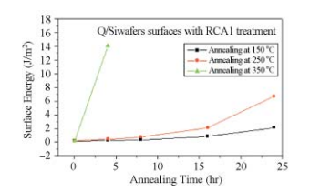
Single-crystalline silicon films have been prepared on synthetic quartz (fused quartz or quartz glass) substrates by ultra-low temperature wafer bonding and thinning approaches. The wafer surfaces treated only by RCA1 process showed a relative low initial bonding energy of 0.17 J/m2. Though the bonding strength can be raised to 14 J/m2 after 350 ℃ annealing for 4 h, the severe warpage of bonded wafer led to the poor total thickness variation (TTV) of SOQ wafers (TTV > 10 m) after thinning. However, if the wafer surfaces treated with RCA1 process, and followed by O2 plasma treatment for 15 sec, the initial bonding energy can be raised to 0.83 J/m2. After the bonded wafer annealed at 100 ℃ for 16 hrs, the bonding strength increased rapidly to 13.3 J/m2 with still a low warpage of 2.5 μm. The SOQ wafers fabricated by the ultra-low temperature bonding, lapping and polishing showed relative good TTV of less than 4 μm.
High carrier mobility single-crystalline silicon film on an insulating quartz substrate (SOQ) is very attractive for the use in microwave devices, image sensor, electro-luminescence displays, solar cells, optical waveguide, microdisplays and MEMS applications. However, it is difficult to directly deposit a single-crystalline silicon layer on a quartz substrate due to the severe lattice mismatch of silicon and quartz materials. Wafer bonding technology could provide a high degree of flexibility in materials integration to solve the lattice mismatch problem. Generally, wafer bonding involves initial bonding (contacting) at room temperature, annealing at relatively high temperature to strengthen the bond and processing one or both wafers of the pairs. However, when bonding dissimilar materials and annealing at high temperature, it would induce thermal stress due to the difference in thermal expansion coefficient (TEC, 2.6 × 10⁻⁶ ℃-1 for Si and 0.5 x 10⁻⁶ ℃-1for synthetic quartz). The thermal stress degrades the material by generating defects. It can also make the wafers crack and completely debond. The thermal stress is proportional to the difference in TEC and temperature (from annealing temperature to room temperature). In order to avoid debonding of the dissimilar wafers, a lower temperature annealing process to strengthen the bond is necessary to be developed. Q.-Y. Tong et al. developed a low temperature (150 ℃) wafer bonding process to prepare the SOQ wafer, but the processing time is over 200 h. The long fabricating time is not suitable for mass production. In this study, an effective method to reduce the processing time was developed using the ultra-low temperature (100 ℃) wafer bonding with O2 plasma treatment of the wafers surfaces before initial bonding.
The wafer surfaces with O2 plasma treatment for 15 vsec showed the highest of initial bonding energy of 0.83 J/m2. The initial bonding energy decreased gradually along with the increase of plasma treatment time. We know that the gas chemistry and plasma parameters (applied power, pressure, plasma density, plasma process time etc.) would influence the plasma/surface interactions. If the wafer surfaces expose in plasma environment for a long time, the bombardment of energetic ions would induce defect formation and may reduce the O-O bond density on wafer surfaces. The exact reason is not clear now and needs to a further investigation.

Fig1
Due to the severe warpage of the bonded wafer after annealing process, local areas of Si layer were disappeared after the thinning process. The total thickness variation (TTV) of this SOQ wafer was over 10 m. Another pair of the bonded wafers which were treated with RCA1 and O2 plasma, annealed at 100 ℃ for 16 hrs, and thinning, was shown in Figure 3(b). Compared with Figure 3(a), the SOQ wafer fabricated in this way showed relatively good TTV of less then 4 µm (Figure 3(b)). From the above results we can conclude that a low annealing temperature for wafer bonding is a key process of making good quality for SOQ wafers. The total processing time is less than 20 hrs and is suitable for commercial applications.
Four inch SOQ wafers have been successfully developed by ultra-low temperature wafer bonding and thinning approaches. The wafer surfaces treated only by RCA1 process showed a relative low initial bonding energy. Though the bonding strength can be raised after 350 ℃ annealing for 4 hrs, the severe warpage of the bonded wafer led to the poor TTV of fabricated SOQ wafers (TTV > 10 m). However, for the wafer surfaces treated with RCA1 and O2 plasma for 15 sec and annealed at 100 ℃ for 16 hrs, the bonding strength raised rapidly to 13.3 J/m2 with still a low warpage of 2.5 μm. The SOQ wafers fabricated by this ultra-low temperature wafer bonding process showed relative good TTV of less than 4 μm.
上一篇: 晶圆级的金刚石纳米和量子技术