The presented fabrication technology enables the direct integration of electrical interconnects during low temperature wafer bonding of 3D MEMS and wafer-level packaging. The fabrication process relies on wafer stacking by hydrophilic direct bonding of plasma activated Si/SiO2 surfaces and the simultaneous interconnection of two metallization layers by eutectic bonding of ultra-thin AuSn connects. This hybrid low temperature bonding and interconnection technology allows for the integration of metal interconnects and multiple materials in stacked MEMS devices. Further, the technology is fully compatible with waferlevel packaging approaches based on through silicon vias (TSV) or CMOS/MEMS integration. The process flow is successfully validated by fabricating test structures made out of a two wafer stack and featuring multiple ohmic electrical interconnects.
There is a growing interest in improving the performance and functionality of MEMS by integrating different materials combined with high-aspect-ratio 3D silicon structures fabricated by wafer stacking. The integration and electrical connection of metal electrodes for actuation and sensing in such devices is challenging and an important factor for cost and reliability issues. Especially, established wafer stacking technologies, based on anodic or fusion bonding, strongly restrict the integration of a metallization before the bonding due to the required elevated process temperatures. Recent advances in 3D integrated circuit (3D IC) technology demonstrated the potential of metal direct bonding for the stacking and interconnection of ICs . This technology involves a demanding planarization process for adequate mechanical and electrical properties. On the other hand, Cu-Cu thermo-compressive bonding requires an annealing at elevated temperatures in order to allow Cu inter-diffusion and grain growth to achieve high enough bonding strength and low number of interfacial voids.
In this paper we present a hybrid low temperature fabrication technology allowing for bonding wafers featuring MEMS structures and metallization layers. One low temperature process is used to locally connect different materials and layers. A strong mechanical bond is performed by hydrophilic direct bonding of plasma activated Si and SiO2 interfaces. The prevailing bonding mechanism is the polymerization of hydroxyl functional groups which form strong covalent siloxane bonds. Simultaneously ultra-thin AuSn contact pads are forming local electrical interconnects between the metallization layers of the two bonded substrates. Since the electrical interconnect is formed by eutectic bonding and reflow of the AuSn metallization, no substrate planarization by CMP is required before bonding. Further, the eutectic AuSn allows for the process temperature not exceeding 300°C.
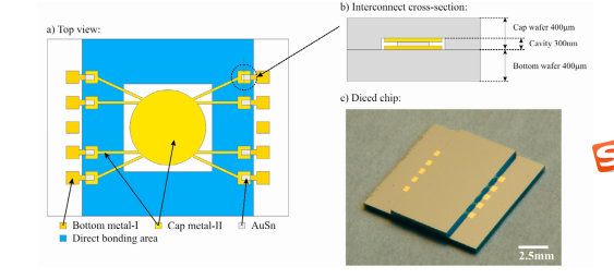
The fabricated test structures are made out of a two wafer stack and are featuring multiple vertical interconnects. The chip-level top view in Figure 1 shows the test device layout (a), an interconnect cross-section (b), as well as a picture of a fabricated chip (c). The basic validation concept is to prepare two substrates with complementary metallizations and interconnecting these by the presented hybrid bonding process. The lower and upper substrates are called bottom and cap wafer, respectively (Fig.1b)). The bottom wafer features the bottom metal-I, which forms the connection pads for the characterization and testing. As shown in Fig.1a), the bottom metal-I forms 8 probing pads per chip. The cap metal-II of the cap substrate constitutes the electrical path, which interconnects all 8 probing pads. Thus, the cap wafer features the cap metal-II as well as the AuSn interconnect metallization, both completely deposited into a 300nm deep cavity. The electrical connection of the bottom metal-I and the cap metal-II takes place by bonding the cap wafer onto the bottom wafer. This is schematically shown in the cross-section of Figure 1b).

Fig1
The process flow is illustrated in Figure 2. For the cap wafer preparation, first alignment markers and cavities for the metallization are structured by ICP dry etching processes (Fig.2a). The isotropic etching of the 300nm deep metallization cavities is time controlled and enables an interconnection by means of thin metal layers and AuSn pads. Then the cap and AuSn metallizations are deposited by e-beam evaporation and structured by a subsequent lift-off process (Fig.2b-c). A white light interferometer (WLI) 3D picture and corresponding profile of a cap metallization with connection line and deposited AuSn pad is shown in Figure 3. The bottom wafer preparation also starts with etching alignment markers and a cavity for the probing pads. This is followed by the deposition and liftoff of the bottom metal-I (Fig.2d).
Then the hybrid low temperature hydrophilic wafer bonding with the local eutectic bonding and reflow of the AuSn interconnects is performed. After the O2-plasma activation for the hydrophilic direct bonding, the bottom and cap wafers are aligned and brought into contact (Fig.2e)). First the eutectic bonding takes place by applying a bond tool pressure of 3 bar at a temperature of 300°C, which is above the eutectic AuSn melting point of 278°C. This step is followed by an extended direct bond annealing at 250°C for four hours (Fig.2f). Finally, a multi-level dicing is performed in order to release the chips and the probing pads for testing (Fig.2g).
上一篇: 超低温晶圆键合和减薄方法的石英晶圆单晶硅
下一篇: 低温氧化铝晶片粘接