Aluminum-aluminum thermo-compression wafer bonding is becoming increasingly important in the production of microelectromechanical systems (MEMS) devices. As the chemically highly stable aluminum oxide layer acts as a diffusion barrier between the two aluminum metallization layers, up to now the process has required bonding temperatures of 300°C or more. By using the EVG®580 ComBond® system, in which a surface treatment and subsequent wafer bonding are both performed in a high vacuum cluster, for the first time successful Al-Al wafer bonding was possible at a temperature of 100°C. The bonded interfaces of blank Al wafers and Al wafers with patterned frames were characterized using C-mode scanning acoustic microscopy (C-SAM) and transmission electron microscopy (TEM) as well as dicing yield and pull tests representative for the bonding strength. The investigations revealed areas of oxide-free, atomic contact at the Al-Al bonded interface.
Thermo-compression wafer bonding is a key technology for the wafer-level production of hermetically sealed cavities, which are essential for the functioning of many microelectromechanical systems (MEMS). Aluminum, with its low material price, high thermal and electrical conductivities and its complementary metal oxide semiconductor (CMOS) compatibility, is a promising candidate for the fabrication of CMOS-MEMS, in which the sensor/actuator part is bonded to the electrical circuit.
In the references listed in TABLE I, typically temperature of 400°C-550°C led to bonded Al-Al wafers with Al2O3 precipitates present at the bonded interface and still with reasonably good bonding quality. In the EVG®580 ComBond® system, the aluminum oxide is first removed physically, followed by bonding of the two metal layers, both performed in a high vacuum cluster. The first Al-Al wafers were successfully bonded at 100°C using EVG®580 ComBond® equipment, which allows for preparation of oxide-free surfaces enhancing atomic contact. Notably, Akatsu et al. used a surface activated bonding set-up (10) to bond cubes of single crystalline aluminum at room temperature (with a bonding pressure of 40 MPa). However, to our knowledge, there is no account for surface activated Al-Al bonding on wafer-level.
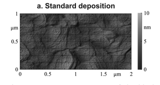
In the present work, Al-Al bonding of blank layers bonded in the EVG®580 ComBond® equipment was compared to Al-Al wafers bonded conventionally in an EVG®520IS equipment. The microstructure of the aluminum films on the silicon substrates was characterized by atomic force microscopy (AFM) and transmission electron microscopy (TEM). C-mode scanning acoustic microscopy (C-SAM), TEM and energy dispersive x-ray spectroscopy (EDXS) interface studies of the Al-Al interfaces bonded with this novel method revealed oxide-free, atomic contact and grain growth across the original interface. Further, the bond strength was characterized based on dicing yield and pull tests of bonded Al-Al wafers with patterned frame structures.

Fig1
The proprietary ComBond® surface preparation process can be tuned to perform an oxide removal while only negligibly changing the sample’s surface roughness. Prior to the bonding experiments, aluminum oxide removal rates of up to 15 nm/min were confirmed by thickness measurements of Al2O3 films on Si substrates. The bonding chamber in the EVG®580 ComBond® equipment is identical in functionality to that of the EVG®520IS used for standard bonds, the major difference is that in this equipment the wafers are handled between the ComBond® surface preparation chamber and the bond chamber under high vacuum environment and not at ambient conditions. In both setups, a bonding force of 60 kN was used. Since these bonded wafer pairs are full area bonds of non-patterned wafers (bonding area: 314 cm2), the applied force corresponds to a bonding pressure of 1.9 MPa.
A wafer with frames was bonded to a flat wafer in the ComBond® system applying a bonding force of 60 kN and a bonding temperature of 100°C or 150°C. The applied bonding force corresponded to a bonding pressure of 114.3 MPa. The bonded wafer pairs were diced into individual dies using a DAD321 (Disco) saw. The dicing yield, defined as the percentage of dies that were not delaminated after the dicing process, was recorded. A random selection of 12 non-delaminated dies of frame type F200R was made from each bonded pair, glued to flat headed bolts and pull tested using a MiniMat2000 equipment (Rheometric Inc.). During pull testing, displacement versus applied force was recorded and the maximum force, at which the fracture occurred, designated as the fracture force, was determined. The bond strength was calculated by dividing the fracture force by the bonding area.
下一篇: 半导体晶片光调制热反射率的两层模型