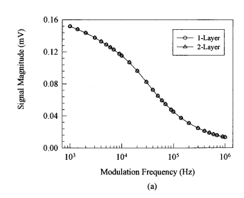
A complete theoretical analysis of the laser photomodulated thermoreflectance signal from a two-layer semiconducting wafer is presented. It is shown that the electronic and thermal properties of a thin surface layer may be determined by using the measured induced photothermal signal. Several numerical simulations are performed in order to study the influence of various electronic, optical and thermal parameters of the two-layer sample on the photomodulated thermoreflectance signal. The influence of the upper layer as well as the influence of the substrate on the signal are also discussed and parameter regimes are identified, where the characterization of the thin overlayer may be possible using this technique.
Laser photomodulated thermoreflectance (PMTR)has been used extensively in recent years for defect diagnostics in semiconducting wafers and several theoretical models have been developed in order to improve the analysis of the results obtained by PMTR measurements.1–3 To render the PMTR technique complete for quantitative analyses, several questions need to be answered, necessitating the development of new models suitable not only for homogeneous but also for inhomogeneous semiconductors. Special attention must be given to thin surface layers which are important for device processing in modern semiconductor technology. For example, the majority of PMTR studies have been performed on implanted semiconducting wafers which constitute a twolayer system: the substrate and the implanted surface thin film. One of the main problems in this field is that monolayer models are mostly used in order to interpret photothermally induced signals obtained from layered wafers.1,4,5 This modeling will likely be unable to exploit small, yet significant, signal features associated with discrete or continuously varying surface layers, especially at high modulation frequencies of the pump laser beam intensity.
Wurm et al.6 developed a two-layer model which can, in principle, be used for quantitative analysis of experimental data obtained from a thin implanted surface layer on crystalline silicon. Unfortunately, thermal wave effects were neglected, as well as any changes with temperature in the thermophysical properties of the optically heated semiconductor, which makes their model inadequate in the case where thermal contribution plays a dominant role, such as with amorphous implanted layers. Nevertheless, using this model, the authors calculated recombination lifetimes of amorphous implanted layers to be of the order of ms, which is too high for amorphous silicon layers.
It is important to note that in the case of thin films the term (1-R) in Eq. is not completely correct. A more precise representation of this term should consider: the incident power at the air-film interface, the reflection coefficient of the interface and the multiple reflections in the various layers. In the present analysis, however, multireflection phenomena and optical interference phenomena are not considered. Such effects are not significant when monochromatic light is used with wavelength outside the range of the thin-film thickness. In the case of implanted surface layers, the absence of a sharp interface between upper layer and substrate precludes the appearance of pronounced interference fringes. Furthermore (Appendix and Ref. 15), the optical interferences, and generally the presence of F, only influence the absolute and not the relative amplitudes of the PMTR signal.

Fig1
The theory and simulations presented in this work show the features and potential of the photomodulated thermoreflectance technique as a complete non-contact and nondestructive quantitative characterization methodology of semiconducting processed wafers with an electronically active overlayer. This model is currently being utilized for quantitative analysis of annealing kinetics of defects in our laboratory. The present modeling on the variation of optical, thermal and electronic properties as functions of the annealing temperature may potentially yield depth-profilometric analysis on long and short-range disorder in processed semiconductors, if the relevant substrate properties are known or can be measured.
上一篇: 低温氧化铝晶片粘接
下一篇: 半导体薄膜化学浴沉积中的基材间距