The precise chemical analysis PCA was developed to study the layers near the semiconductor surface. This method is Ž . based on dissolving of different components in the selective etchants. The solution, containing the products of etching, was analysed with photometric technique. In this paper, we present the photometric measurements of ‘‘free’’ non-intercon- Ž nected Si atoms, which remain at the silicon surface after a typical process of semiconductor technology such as rapid . thermal diffusion RTD of boron into silicon. The advantage of this method is that it is non-destructive for the silicon Ž . matrix. The boron content was also investigated in the volume near the surface. The accuracy is evaluated as 5%. q 2000 Elsevier Science B.V. All rights reserved.
The fabrication of semiconductor devices requires processes such as thermal treatment, lithography and contact deposition, which affect the near-surface structure and composition of the semiconductor material. These process-induced changes can in turn affect the device performance. It has been noted that all structural and composition changes at the surface are accompanied by thermomechanical strains, point defect or atom motion and dislocation Ž . generation. In addition, the grain structure may be modified. Problems with near-surface diffusion in semiconductors have been observed in the past. For example, grain boundary diffusion and its dependence on the degree of disorientation was discussed in Ref. 1 .
In this reaction, doped SiO is formed on the 2 surface of the product wafer and becomes a dopant source for elemental boron, which diffuses into the silicon substrate. Following RTD, the surface composition, and in particular a measurement of the amount of boron and silicon atoms present in a form other than crystalline silicon, was determined using precise chemical analysis PCA 6–8 . Having de- Ž . w x termined the surface composition, it is possible to investigate the effects of grain boundary diffusion, crystal tensile strain and the dynamics of the mechanical stresses in the subsurface layers.
A FEK-56M photometer was used to measure absorbance, with red 720 nm filter and 30-mm Ž . working distance used for Si measurement and orange 10 nm filter and 5-mm working distance used Ž . for B determination. For Si and B, concentrations in the final solution over the range 0.1–1.0 mgrml were measurable, with an accuracy of about 5%. The masses of free Si and B from each processed sample were normalised to the square unit for each process studied.

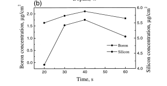
Fig1(b)
The dependencies of boron and silicon concentrations upon the duration of the RTP process are also similar. The semiconductor surface is enriched with silicon and depleted with boron. Atoms flow in two directions during RTD. Firstly, boron atoms diffuse from the surface into the wafer volume, and, secondly, silicon atoms migrate in the opposite direction, from the wafer volume to the surface. Analysis of the curve in Fig. 1b suggests that silicon and boron concentrations show a lightly logarithmic dependence on RTP duration for ‘‘free’’ silicon atoms and for boron in the volume near the surface. It may be shown that the diffusion of silicon atoms occurs under the influence of forces which are determined by the gradient of chemical potential Dm;78 kcalrmol. This is confirmed by the data from Fig. 2a and b. The value of 78 kcalrmol corresponds to the energy of formation destruction of hexagonal sili- Ž . con. This suggests that boron atoms substitute the silicon atoms in the semiconductor during RTP.
上一篇: 半导体薄膜化学浴沉积中的基材间距
下一篇: 晶体硅片上扩散层的光致发光激发光谱