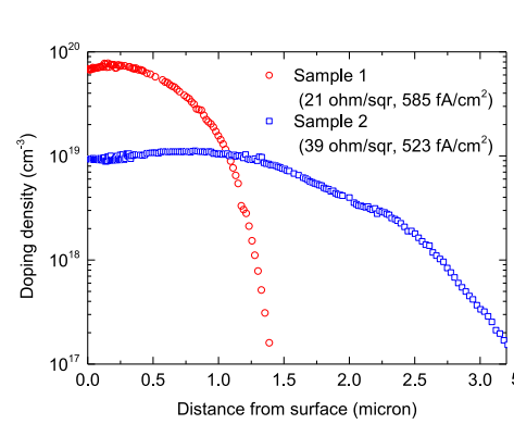
Photoluminescence (PL) excitation spectroscopy is applied to observe the evolution of the luminescence spectra from dopant-diffused crystalline silicon wafers with varying excitation wavelength. Utilizing the micrometer-scale spatial resolution achievable with confocal optics in a micro-photoluminescence spectroscopy system, along with the well-resolved luminescence peaks at cryogenic temperatures from various defects and structures in a single-silicon substrate, we are able to examine the doping densities and junction depths of various boron-diffused wafers, as well as the distribution of defects induced underneath the wafer surface by the post-diffusion thermal treatment. Our conclusions are validated by photoluminescence scans and transmission electron microscopy applied to vertical cross sections, which confifirm the presence of dislocations below the diffused regions.
In this work, we combine the two PL techniques mentioned above (PLS and PLE) and capture the entire band-to-band luminescence spectrum, while varying the excitation wavelength, with the measurements performed at cryogenic temperatures and with micrometer-scale spatial resolution. This spectrally resolved PLE technique is founded on the fact that the radiative recombination mechanism is generally different for each layer or defect type in a c-Si wafer, leading to distinct peaks in PL spectra at cryogenic temperatures. Furthermore, these components of the aggregate luminescence spectrum from a wafer composed of multiple layers are expected to have different dependences on the excitation wavelength, since the fraction of the excitation light absorbed in each layer varies with excitation wavelength. Therefore, by varying the excitation wavelengths, we can probe the layers and defects at different depths below the wafer surface, providing useful information about the spatial distribution of dopants and defects. First, we demonstrate this method on boron-diffused c-Si samples with various doping densities and junction depths. After that, we apply the method to detect and characterize specifific defects induced underneath the wafer surface by the post-diffusion thermal treatment, highlighting some potential applications of the technique for silicon PV. The results are confifirmed by μPLS measurements and transmission electron microscopy (TEM) performed on vertical cross sections of relevant samples.
The samples studied in Section III are flfloat-zone phosphorusdoped c-Si wafers with a resistivity of 100 Ω·cm. They were fifirst chemically etched in a solution consisting of HF and HNO3 to remove saw damage. After that, they were heavily doped with boron from a BBr3 gas source between 900 and 1000 °C in a quartz tube furnace with various drive-in times in a pure oxygen environment to achieve different doping profifiles in the diffused layers. More details about this diffusion process can be found in [30].

Fig1
Finally, a TEM two-beam bright-fifield image of the (0 1 1) cross section of the boron-diffused silicon wafer N3 is shown in Fig. 7(a) and (b) for low and high magnififications, respectively. The micrograph in Fig. 7(a) reveals a dislocation band located about 3 μm below the wafer surface. Between this dislocation band and the surface is a dislocation-free zone. This distribution of dislocations is similar to the results reported by Ning and was explained by the movement of dislocations formed at the wafer surface during the annealing and cooling process. Therefore, the observed deep-level luminescence is likely to be related to the dislocations.
Combining spectrally resolved PL and PLE spectroscopy techniques, we have captured full luminescence spectra with varying excitation wavelengths, allowing us to examine the properties of different layers and defect types at various depths inside boron-diffused silicon wafers. We have demonstrated that this method can be used to qualitatively assess doping concentrations and junction depths. In addition, we have applied this method to detect dislocations induced by the post-diffusion thermal treatment process, giving insightful information about the spatial distribution of both dislocations and secondary defects located below the wafer surfaces.
The authors would like to thank Prof. H. Tan for providing access to the spectroscopic equipment; Prof. B. Luther-Davies, Dr. S. Mokkapati, and D. Llewellyn for assisting with the hardware setup; and D. Yan for providing the boron-diffused n-type silicon wafers. The Australian National Fabrication Facility, the Center for Advanced Microscopy, and the Australian Microscopy and Microanalysis Research Facility ACT node are greatly acknowledged for providing access to some of the facilities used in this work.
上一篇: 快速热处理后硅晶片的精密化学分析开发
下一篇: 用于 MEMS 器件的金属晶圆键合