Metal fifilms can be used as bonding layers at wafer-level in MEMS manufacturing processes for device assembly as well as just for electrical integration of difffferent components. One has to distinguish between two categories of processes: metal thermo-compression bonding on one side, and bonding with formation of an eutectic alloy layer or an intermetallic compound. The difffferent process principles determine also the applications area for each. From electrical interconnections to wafer-level packaging (with special emphasis on vacuum packaging) metal wafer bonding is a very important technology in MEMS manufacturing processes.
Wafer bonding plays an important role in Micro-Electro-Mechanical Systems (MEMS) applications as a technique used for joining substrates. The need to address the large applications variety was the driving force for the development of difffferent wafer bonding processes.
Among the wafer bonding processes currently used for industrial applications can be mentioned direct bonding (also known as fusion or molecular bonding - adhesion is generated by chemical bonds between the molecules on the two surfaces) , anodic bonding (used to bond a Si wafer to a glass wafer - bond appears due to an oxide layer grown at the interface) , adhesive bonding (using intermediate layers, typically polymers), eutectic bonding (bond occurs through an eutectic alloy layer grown at the interface) or intermetallic bonding and thermo-compression bonding (metal bond – bond occurs between two metal surfaces pressed together under heating) .
Physical, chemical, electrical, and thermodynamic properties of the given material play a crucial role in the feasibility of the bond process and must be considered already at the design stage of an application. Wafer bonding process selection is based on various criteria related to the materials used (substrates types, bonding temperature and thermal profifile) as well as to the desired application (type of bond – mechanical connection, electrical or thermal conductivity of interface, optical properties and device working temperature).
Apart from direct (fusion) bonding, processes based on “bonding layers” are extensively used in MEMS manufacturing. The intermediate layers choice is made based on required processing temperatures as well as on other materials characteristics (e.g. specifific outgasing or thermal/ electrical/ optical conductivity).
Some of the main eutectic alloys used for wafer bonding applications are listed in Table 1. For a successful eutectic bonding process it is very important that bonder assures a good temperature uniformity across the entire wafer surface and also to control very well the temperature value (avoid overshooting the set point) in order to have a reliable process.
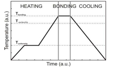
Experimental results showed that good quality bonded interfaces are obtained when temperature is fifirst raised to a value lower than the eutectic temperature, maintained constant to reach uniform heating of both substrates, than increased again to a temperature exceeding the eutectic point with 10–20◦C (depending on specifific process conditions and on substrates restrictions) followed by cooling down to a temperature below the eutectic temperature. Temperature ramp for heating/cooling processes are important and have to be selected based on substrates materials (to avoid thermal shock for dissimilar materials) as well as on device requirements (heating/cooling in vacuum or both or only single wafer in contact with heaters).

Fig1
Eutectic wafer bonding does not require application of high contact force. Due to the liquid phase formed during the process, high contact force results always in metal squeezing out of the interface, resulting in poor interface layer uniformity as well as contamination of the bond tools and bond chamber. The role of the low contact force required is just to ensure good contact of the two wafers and good contact of the two heaters of the bonder with wafers’ back sides.
This bonding process is an advanced type of solder bond that can form highquality hermetic seals at lower temperatures than other bonding technologies. This technique uses one thin metal layer (typically 1–10 µm thick) which during a thermal process inter-diffffuses with its bonding partner forming an inter-metallic compound layer with re-melting temperature higher than the bonding temperature .
In thermo-compression bonding process the two surfaces adhere to each other due to a metal bond established between two metal surfaces pressed together under heating. The bonding mechanism is enhanced by the deformation of the two surfaces in contact in order to disrupt any intervening surface fifilms and enable metal-to-metal contact. By heating the two metal surfaces the contact force applied for the bond process can be minimized due to metal softening. High force uniformity across the bonding area enables high bonding yield.
上一篇: 晶体硅片上扩散层的光致发光激发光谱
下一篇: 直接晶圆键合中空隙的光声成像