We demonstrate photoacoustic thermal imaging of the voids occurring at the interface of directly bonded silicon wafers. The wafers are not touched by probes, minimizing wafer contamination, and the technique does not require the outer surfaces of the bonded wafers to be polished. The method is effective for infrared-opaque materials, as demonstrated by coating a silicon bonded pair with bismuth and obtaining an improvement in the contrast.
Direct bonding is widely used for joining semiconductor wafers without the use of any intermediate layers.1 The basic procedure is to clean the two polished wafer surfaces and bring them into contact, whereupon they bond spontaneously, due both to the van der Waals attraction and to the formation of hydrogen bonds between the OH-terminated surfaces and adsorbed water molecules. During subsequent thermal annealing, water molecules, oxygen, and hydrogen atoms can be eliminated, and covalent bonding across the interface is obtained.
When used to join an oxidized silicon wafer to another silicon wafer, which is later thinned, or from which a thin bonded layer is detached, the method fifinds one of its most important applications, namely the manufacture of ‘‘siliconon-insulator’( SOI)substrates.3 The same method has been used to join surfaces of different materials, including metals, semiconductors, and dielectrics, and therefore to obtain substrates which take advantage of the properties of both materials.
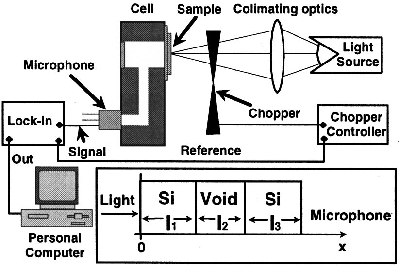
Heat conduction, like sound conduction, is not limited by the optical gap, and therefore can be used for imaging both semiconductors and metals. Photoacoustic microscopy has previously been demonstrated for detection of purposely introduced cavities inside solid samples, and for notches on the back of samples.8 In these cases, the defects had thickness of the order of millimeters, while here we demonstrate detection of voids with submicron thickness. The physics and experimental methods of photoacoustic (PA)characterization are well described in the literature, but we review the basic idea here. The sample surface is illuminated from the front side with intensity-modulated light. The energy absorbed increases the sample local temperature, and heat is transported through the sample by conduction. This heats up the backside of the sample and the flfluid usually air! in the cell facing it, causing a periodic change in pressure which is detected by a microphone.
The imaged region is not touched by any probe, minimizing wafer contamination and risks to the integrity of weak, nonannealed bonds. Other photothermal techniques could be used as well,9 which differ in the method used for measuring the increase in the temperature of the back surface. The PA technique has the advantages of requiring contact of this surface to air only and of having no special requirements of polishing of the exterior surfaces. It also has a signifificant advantage of principle: all the scanning can be done optically, which is a far more robust technique than the mechanical scan used in acoustic microscopy.

Fig1
The samples were imaged by infrared transmitted light, supplied by an incandescent 20 W light bulb, fifiltered by a long-pass fifilter, and the image detected by a near-infrared video camera was captured by a frame grabber. Tests have shown that the interference fringes corresponded to a wavelength distribution centered at l 5 1050 nm. The interfacial distance was determined by attributing a distance between the two silicon pieces corresponding to (2i-1)3 l /4 at the ith dark fringe, with the counting beginning from the region with no fringes.
A small area of each sample was selected for photoacoustic imaging. They were illuminated with white light from a 100 W tungsten–halogen lamp focused to a small square spot, with a Gaussian-like profifile of 480 m m full width at half maximum (FWHM) , and integrated intensity of 4.7 mW. The incident light was modulated by a chopper at a frequency of 17 Hz. The transmitted heat was detected from the backside, using an air-fifilled cell at atmospheric pressure into which an electret microphone was inserted. The periodic pressure variation on the microphone was detected synchronously with the light modulation, using a lock-in amplififier. The cell was mounted on a x-y positioner, so that the light spot could be scanned on the sample. The results shown here were obtained with manual scanning, and limited to a 7 mm by 7 mm region, with 500 m m steps. At each position the amplitude and phase of the microphone voltage were recorded. They were normalized against the signal from asingle wafer sample. The arrangement is shown schematically in Fig. 1.
上一篇: 用于 MEMS 器件的金属晶圆键合
下一篇: 紫外和深紫外二阶非线性光学晶体的最新进展