Thin-fifilm solar cells based on polycrystalline p-type Cu(In1-xGax)Se2 absorbers show the highest power conversion effificiencies (>21%)1 among all thin-fifilm solar cell photovoltaic materials. Typical chalcopyrite solar cells consist of a stack of various semiconductors and metals, consecutively deposited onto glass substrates. In this multilayer architecture, the chemical, structural, and electronic interface properties play a crucial role for the overall performance of the fifinal solar cell device. In this respect, with the goal to improve understanding of the interface formation and properties, and to ultimately improve solar cell effificiencies, a signifificant number of surface and interface studies have been performed in the past, many of those using photoemission spectroscopy or scanning probe microscopy.The conclusions based on the fifindings from these techniques mainly rely on the measurement of clean sample surfaces under ultrahigh vacuum (UHV) conditions. However, for such kind of studies, samples are typically obtained from independent growth equipment and are transferred through air into the UHV of the experimental setup for characterization. Contamination and oxidation can signifificantly inflfluence the results of these characterization techniques. Therefore, it is important to create reproducible and well defifined surfaces with respect to their composition that are free of contamination.
In the past, results on the oxidation of Cu(In1-xGax)Se2 surfaces and their chemical etching have been presented. It was found that etching in NH3- and KCN-based solutions can remove undesired secondary phases and oxides from the surface of Cu(In,Ga)(S,Se)2, as, i.e., Cu-selenides or SeO2. 3,15,16 Kazmerski et al. studied the oxidation of CuInSe2 by controlled oxygen exposure under UHV conditions and the subsequent cleaning using ion etching.An oxidation study of CuGaSe2 was presented by W€urz et al., who compared the oxidation after different exposure times to air. X-ray photoelectron spectroscopy (XPS) was then used to analyze the different oxide phases present at the surface. However, so far, a systematic study of how good wetchemical surface cleaning procedures work for different degrees of surface oxidation is still missing.
Polycrystalline CuIn0.71Ga0.29Se2 layers were deposited onto Mo-coated soda-lime glass substrates by a wellestablished multi-stage co-evaporation process.17,18 In the fifirst step, In, Ga, and Se are evaporated at a substrate temperature of Tsub¼ 330 ℃ resulting in a nominal (In0.71Ga0.29)2Se3 layer composition. During the second step, Cu and Se are deposited at a higher temperature Tsub¼ 530 ℃ Once the stoichiometric point is just passed, i.e., [Cu]/([In] þ [Ga]) > 1, the Cu flflux is turned off. In the third step, In, Ga, and Se are evaporated until a slightly Cu-poor sample composition is reached with values of about [Cu]/([In] þ [Ga]) 0.79.
Immediately after the defifined air exposure, the surface of each sample was wet-chemically treated using KCN- or NH3-based aqueous solutions. The NH3 treatment consisted of dipping the sample in 1.5 mol/l aqueous NH3 solution for 10 s, 100 s, or 1000 s at room temperature. This treatment resembles cleaning processes similar to those occurring during the standard wet-chemical CdS buffer deposition. For the KCN treatment, the CuIn0.71Ga0.29Se2 layers were dipped into 0.15 mol/l aqueous KCN solution for 2 min also at room temperature. After the respective treatments, all samples were rinsed with N2-purged de-ionized water and subsequently dried with N2. The surface treatment of all samples was performed under inert gas atmosphere in a N2-fifilled glovebox with an O2 concentration of ≤1 ppm attached to the UHV chamber of the XPS setup. Therefore, post-cleaning re-exposure of the samples to ambient conditions could be minimized.
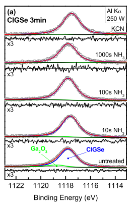
Quantitative analysis of the surface composition was obtained from fifits of specifific photoemission lines of the involved elements. In the following, we present the analysis for each element in the sequence as presented for the qualitative analysis above. The surface content of gallium was analyzed using the Ga 2p3/2 photoemission line (see Fig. 4). As a result of the already discussed presence of Ga2O3 at the CuIn0.71Ga0.29Se2 surface (see above), an asymmetric broadening of the peak towards higher binding energies is expected and can be observed—least prominent for the untreated samples and increasing with air exposure time. Hence, the Ga 2p3/2 line was fifitted by two Voigt functions. Fig. 4 shows the experimental data and the fifits of the Ga 2p3/2 line as a function of the samples exposure time to air and chemical surface treatment.

Fig1
We systematically analyzed the oxidation behavior and the inflfluence of wet chemical surface treatments on polycrystalline CuIn0.71Ga0.29Se2 layers under defifined ambient conditions. For this purpose, CuIn0.71Ga0.29Se2 layers were exposed to air for <3 min, 100 h, or 1000 h, treated with KCN- or NH3-based aqueous solutions, and analyzed using surface sensitive x-ray photoelectron and x-ray excited Auger electron spectroscopy. Quantitative analysis of the photoemission spectra revealed that oxygen primarily reacts with Ga and In. This behavior is well reflflected by the thermodynamic reference data (standard formation enthalpies) of related oxide compounds. Furthermore, the segregation of Cu selenides at the surface of the chalcopyrite could be veri- fified in agreement with literature.2,7,15 This selenide phase can be removed by KCN solution which was confifirmed to be the best surface treatment to produce defifined and reproducible chemical surface conditions. We could show that the KCN treated surface of air-exposed CuIn0.71Ga0.29Se2 layers is in its chemical surface structure – apart from a slight change in surface composition (i.e., Cu defificiency) – identical to a (nearly) non air-exposed surface if exposure is limited to 100 h. This fifinding is not only crucial for the reliable/ reproducible employment of surface science tools to study chalcopyrite surfaces but also needs to be considered for solar cell production in the laboratory and in an industrial mass-production environment.
下一篇: 晶圆对准方法