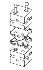
A silicon alignment pin is used to align successive layer of component made in semiconductor chips and/or metallic components to make easier the assembly of devices having a layered structure. The pin is made as a compressible structure which can be squeezed to reduce its outer diameter, have one end fit into a corresponding alignment pocket or cavity defined in a layer of material to be assembled into a layered structure, and then allowed to expand to produce an interference fit with the cavity. The other end can then be inserted into a corresponding cavity defined in a surface of a second layer of material that mates with the first layer. The two layers are in registry when the pin is mated to both. Multiple layers can be assembled to create a multilayer structure. Examples of such devices are presented.
The present application is a divisional application of U.S. application Ser. No. 13/871,830 filed on Apr. 26, 2013 which, in turn, claims priority to and the benefit of U.S. provisional patent application Ser. No. 61/638,939, filed Apr. 26, 2012, and U.S. provisional patent application Ser. No. 61/651,940, filed May 25, 2012, each of which applications is incorporated herein by reference in its entirety.
Submillimeter-wave heterodyne receivers are important for a number of applications, from providing quantitative molecular abundance profiles in atmospheres to detecting contra-band. The current generation of receivers relics on metal waveguide blocks made using conventional precision 45 machining tools such as end mills. For real time imaging capabilities and for large fields of view it is highly desirable to have two dimensional detector arrays, and therefore novel approaches to building compact waveguide architectures are needed.
Micromachining of submillimeter-wave and terahertz circuits is a very attractive approach for terahertz waveguide 55 components since it offers the potential for lower cost and better precision fabrication. See, for example, V. Lubecke, K. Mizuno, and G. Rebeiz, "Micromachining for terahertz applications," Microwave Theory and Techniques, IEEE Transactions on, vol. 46, no. 11, pp. 1821-1831, November 60 1998, Micromachining offers the potential for batch fabrication at photolithographic accuracies, thus reducing the cost per component while improving precision and uniformity. This type of fabrication technology could enable the development of multi-pixel terahertz systems and novel 65 components that are not compatible with CNC metal machining.

Fig1
These resist based technique have some disadvantages. SU-8 processes are very challenging to stabilize and the resist is difficult to deposit uniformly, reducing the precision of each layer thickness or requiring an additional processing step such as lapping. LIGA suffers from similar problems, as electroplating a flat layer of tens to hundreds of microns thick is very difficult, so lapping is also usually required to planarize each layer.
Recent studies have been successful in the fabrication of silicon micromachined components but there is still alack of effective methods to characterize those circuits. In particular, coupling between the micromachined waveguide and standard metal waveguide flanges suffers from misalignment problems due to the difficulty of aligning to non-metal machined waveguide components.
According to one aspect, the invention features an alignment pin having a first end and a second end. The alignment pin comprises a compressible structure having a central axis, the compressible structure having a arcuate surface having a surface roughness of less than tens of microns disposed about the central axis, the compressible structure having an aperture oriented along the central axis defined within the compressible structure, the compressible structure having two opposed projections each oriented in a direction perpendicular to the central axis, the compressible structure configured to assume a relaxed configuration in which the two opposed projections are spaced apart when no mechanical force is applied to the two opposed projections and the compressible structure is configured to assume a compressed configuration upon the application of a mechanical force to the two opposed projections.