Waveguide Technology is widely believed to constitute one of the most promising approaches to realize affordable Augmented Reality (AR) / Mixed Reality (MR) devices combining smallest form-factor with uncompromised image quality allowing for full immersion user experience. Optical waveguides are made from special grade glass wafers. The characteristics of such wafers are directly determining image properties, such as Field-of-View, contrast, brightness, distortion of the image projected into the user’s eye and many more. We are reporting latest advances in measuring and controlling key quality parameters with focus on total thickness variation, optical homogeneity and thickness tolerance of the wafers. We discuss the impact of these parameters on image quality using optical modelling of the waveguides.
Glass wafers are a key component for the optoelectronic industry, commonly used in sensor applications as substrate or as material for wafer level packaging. Other applications include temporary carriers for processing and packaging of advanced semiconductors. Such “conventional” wafers are produced by taking an asmanufactured glass sheet with the chemical composition of alkaline-free TFT display glass or alumino-borosilicate glass. Optically, these materials show a “normal” refractive index of typically nd = 1.50 ± 0.03. A second key specification of glass wafers is uniformity in thickness, characterized by total thickness variation (TTV). Typical values for TTV are in the order of 10 µm; special grades can be selected for some materials with values down to 5 µm.
Emerging Augmented Reality (AR) and Mixed Reality (MR) market is requiring a completely new class of glass wafers: devices based on the so-called waveguide technology – commonly regarded a most promising approach for high image quality but small form factor devices. Devices based on waveguides are developed and produced by companies such as Microsoft, Magic Leap, Vusix, Waveoptics and many more. This technology requires wafers with high refractive index (typically n ≥ 1.6) and index uniformity and reproducibility much smaller than 10-4 . Furthermore, extremely low total thickness variation is required for AR-wafers with typical demands of TTV < 1 µm.
It is not possible to realize such materials using the standard manufacturing approach: the commonly used manufacturing processes for sheet glass, such as overflow fusion, down-draw or float technology are not compatible with the thermochemical properties of a molten high refractive index glass. In addition, the required TTV levels of AR waveguide technology targeting to below 1 µm are not within the reach of these manufacturing processes.
On the other hand, high refractive index glasses are well established in the optical industry. In addition, the use of plano-plano-polishing to manufacture glass substrates from optical glass was known in the past. However, requirements on total thickness variation for wafers used in Augmented Reality waveguides exceed the specifications of “normal” glass wafers by a factor of 10 as shown by light-guide modeling and experimental investigations.

Fig1
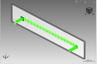
High quality modeling requires also the inclusion of detrimental higher grating orders with accurate grating modeling. In the outcoupling region, the so-called eyebox, per FOV mode, that is a plane wave with one direction, generates various partially overlapping modes, which are generated by splitting at gratings on the path through the light guide. Dependent on the light source these modes are partially coherent to each other, which must be included in the modeling. That finally requires a correct modeling of the interference of the split modes per FOV in the eyebox and for the PSF/MTF calculation.
High index-glass wafers were produced out of blocks of optical glasses using sawing techniques for slicing, and plano-plano polishing processes for reaching specified thickness and surface properties like roughness. The homogeneity of the bulk material is investigated by interferometric means with high accuracy using glass blocks utilizing “polished sample” method. Respective result are shown in Figure 3 obtained at a block of optical glass.
上一篇: 晶圆对准方法
下一篇: 纳米电子学的硅表面和界面问题