To a large extent, the silicon revolution is based on the wonderful properties of the silicon/silicon dioxide interface. The importance of this structure has been documented and cited in many articles and books on the history of technology.1-3 Clearly, it is the most important materials interface in current process technologies.
Briefly, oxidation of silicon results in a large bandgap, uniform, dielectric layer of amorphous SiO2, with the proper band-offsets to allow both p- and n-channel devices to be fabricated. Most important, modern growth and annealing techniques result in interface defect levels that are sufficiently small so that carrier transport is close to theoretical limits expected for SiO2. These excellent qualities have served the community well and been preserved as the basic metal-oxide-semiconductor field-effect transistor (MOSFET) device has scaled down over the last four decades.
Research in the last twenty years has exploited almost every conceivable surface/thin-film probe to establish the underlying physical nature of this critical solid-state interface. Of particular interest has been the nature of the starting silicon surface, the kinetics of the oxidation process, the structure and solid-state chemistry of the silicon-silicon dioxide interface and the relationship of the structure to the electronic properties.
Until recently, our understanding of the growth processes was captured in the Deal-Grove model of oxidation, based on oxygen diffusion and interface reactions.4 Many studies have shown that this model in not a good representation of growth at the modern scale of -2 nm, and an atomic level description is required.
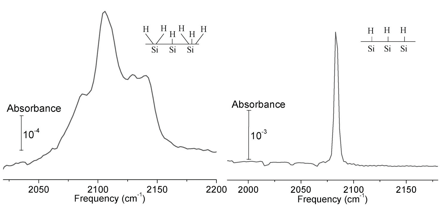
An important aspect of wet processing is the potential control of the surface morphology via preferential etching. A beautiful illustration comes from buffered HF etching of Si(111) and Si(100), which makes it possible to slowly etch silicon after the oxide is removed. Such etching is highly preferential, leading to the formation of atomically flat monohydride-terminated Si(111) surfaces 13 and atomically rough, multihydride-terminated Si(100) surfaces (Fig. 1). Similar behavior is observed for etching of H-terminated silicon in hot water14 and in KOH solutions.
Oxidation of a hydrogen-passivated silicon surface is emerging as an industrially critical area.19 Generally, the barriers for oxygen insertion are much higher, particularly for H2O oxidation,18,20 and the surface oxide structures are stabilized by hydrogen similar to H2O oxidation of clean Si. But the nature of the oxidation is similar, with formation of highly oxygen-coordinated structures involving only the top double layer.

Fig1
Many oxynitridation/nitridation methods have been employed including thermal growth in N2, NO, N2O, NH3 as well as metallorganic chemical vapor deposition (MOCVD), rapid thermal (RT)CVD, plasma-enhanced (PE)CVD, jet vapor deposition (JVD), and atomic layer (AL)CVD.23 In addition to these growth techniques shallow N implants into silicon can be incorporated into a grown oxide with some of the same benefits. Both the gas phase and solidstate chemistry of the nitridation process may be complicated. For example, gas-phase N2O at high temperature rapidly decomposes to its main equilibrium constituents of NO, O2, and N2. Because this may occur during the actual expo- , this may occur during the actual expo- , sure, the dynamics of growth may be strongly time dependent. In the solid state there is evidence that oxygen atoms can remove nitrogen through an exchange mechanism, to form the more thermodynamically stable SiO2. That exchange (and out-diffusion) is more probable near the vacuum surface than the lower interface is part of the explanation for the accumulation of nitrogen at the silicon/dielectric interface, a fortunate circumstance!
The silicon-based roadmap (International Technology Roadmap for Semiconductors, ITRS), provides a pathway for silicon-based technology until ~2020. Success is heavily dependent on new materials and the gate dielectric layer (and gate electrode) is one of the most critical issues. Whether grown by MOCVD, MBE, ALD, or thermally, ultrathin dielectric films can be achieved only with the highest control of the initial surface chemical configuration and the process itself. This will be accomplished through the tools and techniques of surface science and the creativity of materials scientists.