Among various wet cleaning methods, megasonic and jet spray gained their popularity in single wafer cleaning process for the efficient removal of particulate contaminants from the wafer surface. In the present study, we evaluated these two cleaning methods for particle removal efficiency (PRE) and pattern damage on the aluminum layered wafer surface. Also the effect of CO2 dissolved water in jet spray cleaning is assessed by measuring PRE. It is observed that the jet spray cleaning process is more effective in terms of PRE and pattern damage compared to megasonic cleaning and the mixing of CO2 in the water during jet sprays further increases the PRE. We believe that the outcome of the present study is useful for the semiconductor cleaning process engineers and researchers.
In the present study, we evaluated megasonic and jet spray cleaning methods for cleaning aluminum layered wafer surface for their particle removal efficiency (PRE) and pattern damage if any. Sonic waves with frequency of approximately 1 MHz are directed from transducer array panels to the wafer. We also demonstrated the addition of CO2 in DI water changes the pH of DI water and hence enhance the cleaning performance.
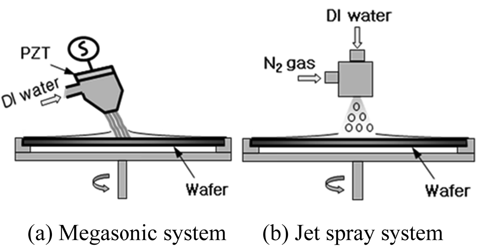
Dynamic random access memory (DRAM) aluminum layer wafers (300 mm in diameter) were used to analyze and to compare the PRE during both megasonic (D-SONIC, SEMES) and jet spray (S-SPRAY, SEMES) cleaning methods. We used metal line formation process which is a part of commercial semiconductor manufacturing process to contaminate the wafers. Aluminum film of thickness of 600 nm can be formed using this process. However, during this process the wafer surfaces are contaminated by random generated dust particles from the chamber wall or suspended dust particles in transport system. The reason we used this deposition process is to achieve actual contamination condition during manufacturing process instead of colloid doping on the bare wafer. The schematic of both wet cleaning process is depicted on the Fig. 1. The operating frequency in megasonic is 1 MHz, and jet spray operates based on 50 and 60 lpm (liter per Minuit) of N2 flow. These flow parameters are as per commercial semiconductor manufacturing process.
We evaluated the effect of CO2 during jet spray cleaning process on a strip patterned wafer. The pattern for damage experiments was prepared by photo lithography and images are depicted in the Fig. 2. These patterns were formed by lithography and etching process after poly-SiO2 film deposition on the poly-Si coated bare wafer. One cell consists of the same shaped 12 patterns with 50 nm~180 nm of pitch sizes and exists in both vertically and horizontally. As 75 cells are formed on a single wafer, the total numbers of patterns are 1800 EA (12×2×75). The depth of the pattern is 420 nm and pitch sizes are 50 nm~180 nm. Thus the aspect ratio of pattern ranges from 1:8 to 1:2. The current (I) flow through all (1800 EA) strip pattern, which is a measure of pattern damage, was recorded to estimate the number of pattern damaged patterns. It is known that the pH of DI water used in jet Spray can affect the particle removal process, hence we monitored the pH of DI water with and without CO2 gas using pH meter (PH1500, EUTHEC) during jet spray cleaning process.

Fig1
Dynamic random access memory (DRAM) aluminum layer wafers (300 mm in diameter) were used to analyze and to compare the PRE during both megasonic (D-SONIC, SEMES) and jet spray (S-SPRAY, SEMES) cleaning methods. We used metal line formation process which is a part of commercial semiconductor manufacturing process to contaminate the wafers. Aluminum film of thickness of 600 nm can be formed using this process. However, during this process the wafer surfaces are contaminated by random generated dust particles from the chamber wall or suspended dust particles in transport system. The reason we used this deposition process is to achieve actual contamination condition during manufacturing process instead of colloid doping on the bare wafer. The schematic of both wet cleaning process is depicted on the Fig. 1. The operating frequency in megasonic is 1 MHz, and jet spray operates based on 50 and 60 lpm (liter per Minuit) of N2 flow. These flow parameters are as per commercial semiconductor manufacturing process.
The number of particles on the wafer was measured before and after each cleaning process with defect analysis system (AIT, KLA-Tencor Co.). Particle count measurements performed using an AIT provides the information of under layer particles, scratches and fallen (lose) particles. The particles morphology is classified using scanning electron microscope (SEM). The chemical compositions of the particles were analyzed using energy dispersive X-ray microanalysis (EDX, RS- 4000 Hitachi).