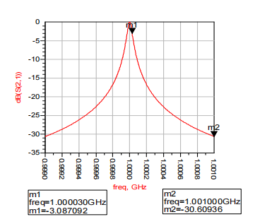
A miniature SAW device is designed and fabricated at 1 GHz for wireless communication system. A 5 m thin film of ZnO is successfully deposited using RF sputtering technique on PECVD SiO2 layer of 1µm on top of Si wafer under various operating conditions. The c-axis oriented ZnO film exhibit a sharp diffraction peak corresponding to the (002) reflection at 2θ=34.42. The fabrication process utilizing the MEMS technology of the SAW device is described. Simulation of the RF SAW filter is performed. Measurements and experimental work are presented for the RF SAW device.
The realization of miniature RF-SAW device on CMOS substrate for mobile and wireless communication system has become very important in recent years. Acoustic wave propagation along the surface of a piezoelectric material provides a means of implementing a variety of signalprocessing devices at frequencies ranging from several MHz to a few GHz. The IDT provides the cornerstone of SAW technology. Its function is to convert electrical energy into mechanical energy and vice versa, for generating and detecting the SAW. The central frequency of a conventional SAW filter is determined by the width of the IDT finger d and the phase velocity which excite the SAW on the piezoelectric materials. Reducing the width of the IDT finger or choosing the piezoelectric material with a higher SAW phase velocity can increase frequency of operation into the GHz range. The SAW wavelength λ (λ =4d) is given by the ratio υ / fo. Where υ the velocity of a SAW wave on a piezoelectric substrate depends on the material and fo is the central frequency. The sensing action of such transducers involves any influences that will alter the acoustic wave velocity υ and, consequently, the associated properties of the wave, such as frequency and time to travel between the sensor and the detector.
In order to achieve good SAW performance, the piezoelectric films should have a smooth surface morphology, sharp interface, and perfect c-axis texture. It is also important that the SAW filter reveals high phase velocity and large electromechanical coupling coefficient as the thickness of piezoelectric film increases. ZnO has a high piezoelectric coupling coefficient, which can be used in surface and bulk acoustic wave devices. ZnO films have been deposited on Si and SiO2/Si, GaAs, and sapphire (Al2O3) substrates. Si and GaAs substrates are of interest for the integration of SAW devices with the main stream microelectronics technology. So these types of devices can be implemented with micro-electro-mechanical systems (MEMS) compatible with CMOS technology.
In this work a miniature SAW filter of 1 µm input/output IDTs of 30 pairs is designed and fabricated on 5 µm thin film of ZnO substrate with a center frequency of 1GHz. ZnO film is grown on SiO2/Si substrates by RF sputtering technique. The growth process is optimized to obtain highly oriented ZnO film with a smooth surface morphology. The structural properties of the films are investigated using Xray diffraction. High quality ZnO thin film has been achieved, which are needed for fabrication of low-loss SAW filter. Characterization of the RF SAW device as a transmitter and receiver filter is performed. Measurements and experimental results are presented for the RF SAW filter.

Fig1
The measured results show that the velocity and electromechanical coupling coefficient are strongly influenced as the thickness of ZnO is increased. There are many factors that the central frequency of a conventional SAW filter is determined. Those are the IDT geometry, and the velocity of piezoelectric substrate material. Recent advances in MEMS and NEMS make it possible to reduce the electrode width to submicron and fabricate a multilayer piezoelectric structure. Also increase the thickness of the piezoelectric layer in SAW devices.
This work has received primary funding from the NSF Directorate for Engineering, Division of Electrical and Communications Systems. Additional funding and support has been provided by ERI. We would like to thank Prof. Dr. Ayman El-Dessouki, president of ERI for supporting this work in the Central Electrical and Electronics Research Inst.,CEERI , India. We thank Eng. Sherief Saleh for his assistance in this work, and Dr. S. Ahmed from CEERI. for providing the MEMS facilities.
上一篇: 提高太阳能光伏板效率的清洁和预防过程概述
下一篇: 具有抗反射涂层玻璃的晶体硅光伏组件