In the semiconductor industry, with increasing requirements for high performance, high capacity, high reliability, and compact components, the crack has been one of the most critical issues in accordance with the growing requirement of the wafer-thinning in recent years. Previous researchers presented the crack detection on the silicon wafers with the air-coupled ultrasonic method successfully. However, the high impedance mismatching will be the problem in the industrial field. In this paper, in order to detect the crack, we propose a laser generated Lamb wave method which is not only noncontact, but also reliable for the measurement. The laser-ultrasonic generator and the laser-interferometer are used as a transmitter and a receiver, respectively. We firstly verified the identification of S0 and A0 lamb wave modes and then conducted the crack detection under the thermoelastic regime. The experimental results showed that S0 and A0 modes of lamb wave were clearly generated and detected, and in the case of the crack detection, the estimated crack size by 6 dB drop method was almost equal to the actual crack size. So, the proposed method is expected to make it possible to detect the crack in the silicon wafer in the industrial fields.
Semiconductors have been applied to many fields including smart TVs, smart phones, smart PCs, automobiles, home appliances, and laptop computers. These fields have demanded that the semiconductor should be of high performance, high capacity, high reliability, small components, and low cost. Because of these demands, semiconductor fabrication processes have focused on the lithography for a nanometer-scaled line width. And especially, semiconductor packaging processes have focused on a few trends in recent years: multistacking components and thinner wafers. The multistacking component implies that more chips have to be stacked up within the same size component for the high capacity, and the thinner wafer indicates that wafer thickness has to be very thin up to 30 μm for the multistacking component. Moreover, an attempt to change from 12 inch-wafers to 18 inch-wafers is recently going on, since larger wafers which are able to put more chips have impact on the yield improvement. Because of these trends that wafers are getting thinner and larger, silicon wafers are vulnerable to cracks during manufacturing. The cracks can also lead to the yield drop and reliability failure. Therefore, one of the most critical issues in the semiconductor packaging process is the crack. So, the online crack detection in silicon wafers is becoming more important than ever before and its importance cannot be stressed enough.
Previous articles about the online crack detection which deals with poly-crystalline silicon wafers commonly used in the solar cell industry are largely classified into two groups. One is the contact method by resonance ultrasonic vibrations and impact tests . The other is the noncontact method by an air-coupled ultrasonic lamb wave. Resonance ultrasonic vibrations method can accurately detect the millimeterlength cracks and the impact testing method can also analyze defective wafers. But both of them are driven by external forces which are not adequate for thin silicon wafers under 100 𝜇m thickness used generally. Air-coupled ultrasonic lamb wave method demonstrates the crack detection successfully and lamb wave is suitable for the thin silicon wafer. However, this method has the problem of high impedance mismatches which cause dissipation of most incident energies from the surface of materials. This is also not satisfied for very noisy environment caused from facilities or manufacturing machines.

Fig1
For many years, laser-ultrasonic technology has been increasingly used for nondestructive crack detections. The biggest advantage of this technology is noncontact without regard to external forces and surface conditions of materials. This technology has another advantage that can reduce the energy loss by adjusting the shape of the laser beam for the energy enhancement. Although laserultrasonic technology has these advantages, few studies have performed for the crack detection in silicon wafers.Therefore, we propose the laser generated lamb wave method, which not only is noncontact but also guarantees the reliable measurement. And this paper deals with single crystalline silicon wafers commonly used in the semiconductor industry other than previous papers which deal with poly-crystalline silicon wafers.
Laser-ultrasonic technology has two main regimes. One is thermoelastic regime and the other is ablation regime. In the case of thermoelastic regime, the ultrasonic waves are generated from thermoelastic expansions of materials. Meanwhile, in the case of ablation regime, the ultrasonic waves are generated from the material removal. If the ablation regime is applied to silicon wafers, they will be damaged. So, thermoelastic regime has to be applied to silicon wafers in terms of the reliability. And also there are two possible generation mechanisms; thermal effect and electrostriction. However, the thermal effect is dominant at the high power input while the electrostriction is dominant at the low power input. In our case, the input power was in the range of high power input, so that we did not consider the electrostriction effect.
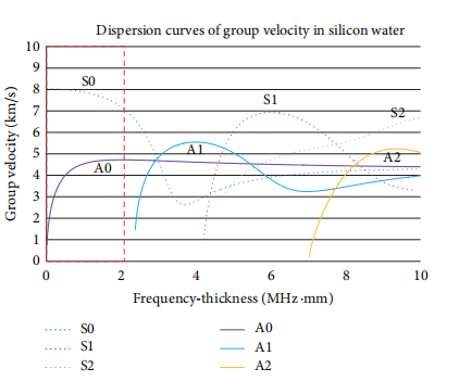
Lamb wave is dispersive, which implies that the wave velocity is dependent on the frequency. So dispersion curves need to be analyzed first. The wave velocities in single-crystalline silicon wafers are listed in Table 1. The silicon wafer has three kinds of different velocities depending on the orientations. But, since wafers have the characteristics that cracks are easily initiated and cleft in the (110) orientation, it is reasonable to consider only the (110) orientation in terms of easier experiments. Figure 1 shows dispersion curves of group velocity which are plotted from velocities at the (110) orientation in the silicon wafer whose thickness is 525 𝜇m. The curves in the dotted box area are mostly used for the practical applications, because other areas are more complicated. So the curves in this box area are supposed to be used for our experiments as well.
上一篇: 高功率脉冲磁控溅射的金属氧化物的反应性
下一篇: 兆声波清洗过程中硅片图案化上的理论计算