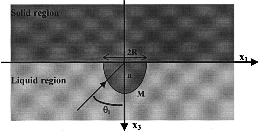
We have calculated, theoretically, the acoustic pressure fifield around a linear pattern on a silicon wafer immersed in water subjected to a megasonic beam. The method of calculation is based on a Green’s function formalism. The acoustic force applied on the pattern by the pressure fifield is determined as a function of frequency and the angle the incident megasonic beam makes with the wafer surface. The calculation is applied to two types of features that may be encountered in megasonic cleaning of integrated circuits prior to packaging, namely a micron-size silicon ridge and a metal wire ~ tens to hundreds of microns in diameter! bonded on a silicon substrate. The calculated acoustic shear stress is found to be orders of magnitude smaller than the shear strength of the features.
Megasonic waves have been extensively used to remove contaminant particles from silicon wafers during manufacturing of semiconductor devices. In this process, planar silicon wafers are immersed in a water-based flfluid solution and subjected to a beam of sonic energy with frequency in the range from 600 kHz to 1 MHz. There has been interest in cleaning nonplanar patterned wafers (for instance vias cleaning) with megasonic waves. However, little is known about the potential damaging effects that the acoustic energy may have on the integrity of the pattern. Several physical processes associated with acoustic cleaning such as microcavitation, acoustic streaming, and acoustic pressure force may have a detrimental impact on the patterned wafers.
Microcavitation is produced by the pressure variations in sound waves moving through the liquid. Cavitation bubbles are formed by the low-pressure component of the acoustic wave. A cavity implodes when the walls can no longer sustain the compressive forces thus transferring energy from the cavity to the surrounding medium. Cavitation is ubiquitous in ultrasonic cleaning systems. In ultrasonic cleaning (with frequencies in the range from 17 to about 100 kHz) , cavitation is known to damage the wafer surface, and ultrasounds are typically avoided in wafer processing. Megasonic cleaning is similar to ultrasonic cleaning but it uses higher frequencies on the order from 600 kHz to 1 MHz. It had been believed that the short time between megasonic pulses on the order of 1–1.25 ms, does not promote the formation of cavities and may therefore lead to less wafer damage.1 More recently, cavitation was detected in a megasonic tank by sonoluminescence.2 These experimental measurements however indicate that the maximum cavitation intensity occurs near the water surface of the megasonic tank.

Fig1
Experimental studies on the effect of megasonic cleaning on wafer damage will therefore be clouded by the superposition of the processes brieflfly discussed above. An experimental investigation of megasonic cleaning is further complicated by the very small spatial and temporal scales at which some of these processes take place. We have therefore elected to undertake a systematic theoretical investigation of these various processes aimed at identifying which one may be detrimental to the integrity of patterned wafers during cleaning. It is the purpose of this article to shed light on the potential damage the oscillatory acoustic pressure fifield of the megasonic wave may inflflict on a patterned wafer. For this, we analyze the interaction between an incident acoustic wave and a silicon substrate supporting a raised linear feature. A methodology based on Green’s functions has been developed to calculate the acoustic fifield around the feature (or surface defect). The acoustic pressure fifield is then integrated over the surface of the defect to calculate the acoustic force on the defect and, in particular, its components along and perpendicular to the wafer surface. We show that the acoustic force varies with the angle of incidence of the sonic beam as well as the frequency of the sound wave. Only the component of the acoustic force tangential to the surface of the wafer exhibits a strong dependence on the angle of incidence and frequency in the range of frequencies used in megasonic cleaning.
We apply the model to the calculation of the acoustic force on two types of raised linear features with signifificantly different sizes that may be encountered in megasonic cleaning of integrated circuits. The fifirst feature is a micron-size silicon ridge on the silicon substrate while the second one consists of a thin metallic wire bonded on a silicon wafer with diameter in the tens to hundreds of micron. A comparison between the calculated acoustic stress in the silicon linear defect and the adhesion strength of raised silicon features on silicon wafers suggests that the acoustic force cannot lead to the damage of silicon features on silicon patterned wafers. Similar conclusions are drawn for the effect of a megasonic wave on metallic wires bonded on a substrate. The acoustic shear stress can be larger in this case (in particular for large diameter wires) than for the micron-size silicon ridge. The maximum shear strength of bonded metal wires exceeds the acoustic stress by more than one order of magnitude and damage of the bonded wires is quite improbable. The acoustic wave may, however, have a damaging effect only for poor quality bonds with very low shear strength.
上一篇: 用激光产生的兰姆波检测单晶硅晶片的裂纹
下一篇: 损失最小的超薄等离子硅晶片太阳能电池