Metal Deposition or metallization process is one of the processes in fabricating a wafer. A wafer is a thin slice of semiconductor material, such as a silicon crystal, used in the fabrication of integrated circuits and other micro-devices. Due to the nature on the process, it creates lot of particles, which would impact the next process if it were not removed. Particle deposition on the wafer surface can cause the circuit to malfunction; leading to a loss of yield. Cleaning process needs to be done after metal deposition process in order to remove the particles.
Metal deposition, which has been constructed by several metal layers, allows the flow of current between interconnections. Each metal layers consist of three types of metal films such as Ion Metal Plasma Titanium (IMP Ti), Titanium Nitride (TiN) and Aluminum. The metal deposition started after the wafer has completed the “Tungsten Chemical Mechanical Polishing” (CMP) process.
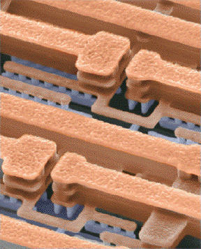
Metal layers are deposited on the wafer to form conductive pathways. The most common metals include aluminium, nickel, chromium, gold, germanium, copper, silver, titanium, tungsten, platinum and tantalum. Selected metal alloy also may be used. The metal layer is shown in Figure 1 and the interconnection between metal layers is shown in Figure 2.
The deposited metal(s) offers special functionality to the substrate. Typically, the metal aqueous solution is employed for the wet metal deposition process due to the consideration of its low cost and operation safety.
In this chapter, a thorough investigation was carried out to improve shut down event problem at Metal Deposition process during wafer fabrication. Particle contamination on wafer surface can cause the circuit to malfunction and leading to machine shut down. Data of shutdown event versus sputter target life showed that the rate of machine shutdown increased by the increment of sputter target life. The sputter target life was further investigated to determine the appropriate sputter target life to be used in order to avoid particles generation during metal deposition process.

Fig1
In this chapter, a thorough investigation was carried out to improve shut down event problem at Metal Deposition process during wafer fabrication. Particle contamination on wafer surface can cause the circuit to malfunction and leading to machine shut down. Data of shutdown event versus sputter target life showed that the rate of machine shutdown increased by the increment of sputter target life. The sputter target life was further investigated to determine the appropriate sputter target life to be used in order to avoid particles generation during metal deposition process.
Particles can be defined as “suspension of solid or liquid mass in air”. Particles can originate from a variety of sources and possess a range of morphological, chemical, physical and thermodynamic properties. The particles could be combustion generated, photo-chemically produced, salt particles from sea spray or even soil-like particles from re-suspended dust. Particles may be liquid; solid or could even be a solid core surrounded by liquid.
Particle contamination can be defined as the act or process of contaminating by particulates. Particle contamination is problematic for many industries. They can appear unexpectedly mixed in solids, liquids and gases. Particles can be from many sources i.e.- metals, biological (skin, hair etc), polymers, building dusts etc. They all have different characteristics and properties such as shape, size and chemistry, which assist in identification. Scanning Electron Microscope (SEM) and Energy-dispersive X-ray spectroscopy (EDX) coupled with optical microscopy provides a powerful machine for unambiguously identifying such particles. The technique is frequently coupled with Fourier transform infrared spectroscopy (FTIR) when identifying the source of organic contamination (Stephen, 2010).