A new generation of power electronic semiconductor devices are being developed for the benefit of space and terrestrial harsh-environment applications. 200-600 V lateral transistors and diodes are being fabricated in a thin layer of silicon (Si) wafer bonded to semi-insulating 4H silicon carbide (SiC) leading to a Si/SiC substrate solution that promises to combine the benefits of silicon-oninsulator (SOI) technology with that of SiC. Here, details of a process are given to produce thin films of silicon 1 and 2 µm thick on the SiC. Simple metal-oxide-semiconductor capacitors (MOS-Cs) and Schottky diodes in these layers revealed that the Si device layer that had been expected to be n-type, was now behaving as a p-type semiconductor. Transmission electron microscopy (TEM) of the interface revealed that the high temperature process employed to transfer the Si device layer from the SOI to the SiC substrate caused lateral inhomogeneity and damage at the interface. This is expected to have increased the amount of trapped charge at the interface, leading to Fermi pinning at the interface, and band bending throughout the Si layer.
A novel silicon-on-silicon-carbide (Si/SiC) power device is being designed and fabricated, conceived to be both radiation hard and able to operate in extreme temperatures, both high and low. This is being produced specifically for space power conversion applications such as electric propulsion and high voltage transmission, where efficient and, potentially, uncooled electronics could increase the overall lifetime, reliability, and science capability of a mission.
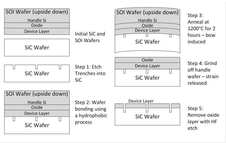
100 mm Si/SiC wafers were fabricated by wafer bonding Norstel semi-insulating (≥ 1.107 Ω-cm) on-axis 4H-SiC to IceMOS Technology Ltd SOI with a buried oxide 2 µm thick, and a lightly ndoped device layer (5 - 45 Ω-cm). Wafers have been produced with a device layer thicknesses 1 and 2 µm thick. The full process used to develop the wafers can be seen in Figure 2.
Initial trials at IceMOS Technology Ltd, directly bonding the two virgin wafers via a number of hydrophilic and hydrophobic methods all resulted in either the handle wafer shearing under the strain, or in a high density of voids, visible in the hydrophobic bonded wafers in the inset to Figure 2. The problem of the voids was suspected to be the result of outgassing while the layers were undergoing a long high temperature anneal to form a permanent bond between the wafers. To overcome this problem, the first step taken in the bonding process (Figure 2) was to etch a grid of trenches 2 µm deep into the SiC surface prior to bonding, giving any gas an escape route during annealing. Next, after a proprietary surface plasma treatment, a hydrophobic bonding process was performed to form a temporary bond between the wafers. A 2 hour, 1200°C anneal was then performed to form a permanent bond between the wafers, and to remove an interfacial oxide, as shown previously in. During annealing, the lattice mismatch between the materials caused a visible bow, the Si side of the wafer being convex. However, this still allowed, in the fourth step, for the Si handle wafer to be ground away down to the oxide layer, releasing the strain. Finally, the oxide, which had been the buried oxide of the SOI wafer, is simply removed with hydrofluoric acid.
Transmission Electron Microscopy (TEM) imaging of the Si/SiC interface revealed the suspected reason for the change in polarity of the Si device layer. In areas, such as Figure 5 (top), a perfectly homogeneous interface was found with no interfacial oxide. In other places, a 1 nm amorphous layer is seen, presumed to be SiO2. Furthermore, in places, features such as those seen in Figure 5 (bottom) are seen, where these are presumed to be pits or voids. This inhomogeneous interface is likely the source of significant charge trapped at the interface. This has been shown in [7] at the Ge/SiC heterojunction to cause Fermi-level pinning, and hence a conduction band offset very different from that expected. Here, it is expected that a high density of interfacial charge causes band bending, which in such a thin, lightly doped Si layer inverts the doping polarity of the entire layer resulting in the p-type behaviour witnessed.

Fig1
The results presented detail an on-going project to fabricate lateral power devices for space applications, using a novel Si/SiC substrate that better deals with the effects of self-heating and radiation. The process used to form the Si/SiC substrate employed a high temperature anneal to remove or reduce any oxide at the heterojunction interface. This is believed to have resulted in an inhomogeneous and damaged interface that will likely have increased the charge residing at the interface. Electrical results on the wafers showed that as a result, the same Si device layer, once transferred onto the SiC had completely changed its polarity from n-type (𝑁𝐷 = 7 × 1014 cm-3 ) to ptype (1.9 × 1015 cm-3 ).
上一篇: 智能传感器的晶圆级真空封装