In this study, a new technique of selective microcap bonding for packaging 3-D MEMS (Micro Electro Mechanical Systems) devices is presented. Microcap bonding on a selected area of the host wafer was successfully demonstrated through flip chip and wafer level alignment. A passivation treatment was developed to separate the microcap from the carrier wafer. A thick metal nickel (Ni) microcap was fabricated by an electroplating process. Its stiffness is superior to that of thin film poly-silicon made by the surface micromachining technique. For the selective microcap packaging process, photo definable materials served as the intermediate adhesive layer between the host wafer and the metal microcap on the carrier wafer. Several types of photo definable material used as the adhesive layer were tested and characterized for bonding strength. The experimental result shows that excellent bonding strength at low bonding temperature can be achieved.
With recent trends in microelectronics moving more and more towards incorporation with MEMS devices, reducing the overall cost becomes vital. One major cost driver in today’s MEMS is the packaging process. Packages for microdevices have all the same functions as for ICs but are considerably more complex. Since MEMS include moving structures, requirements for packaging of such components must take that into account. Some functions also include interaction with the surrounding environment, such as pressure sensors. Packaging should provide mechanical support to the sensitive chip.
MEMS packaging includes microfabrication and wafer bonding processes. There are several wafer bonding techniques offering permanent wafer protection, such as anodic and fusion bonding. Most of these methods use a glass or silicon wafer as a passive lid over the MEMS structures. Cavities between the top lid and the MEMS wafer allow the device structures to move freely. But conventional anodic and fusion wafer bonding techniques can not be employed in all MEMS and IC packaging processes due to high temperature or high electric fields during the bonding process, which might damage IC or MEMS devices. These problems have prompted researchers to study low-temperature bonding techniques , and use eutectic bonding.

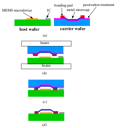
Fig1
In order to accomplish these goals, in this study an innovative wafer bonding process is proposed. It includes using flip chip and wafer level alignment to batch fabricate to lower the manufacturing cost, fabricating a microcap to protect MEMS devices, developing a passivation technique to transfer the microcap to the selected area of the host substrate, offering a lower bonding temperature and an electric field-free bonding process to protect the IC and MEMS devices from damage, and exploring various photo definable materials to find the highest bonding strength. The process flow chart of wafer level bonding using flip chip packaging is shown in figure 1. Photo definable material with patternable characteristics served as the bonding adhesive layer between the microcap and host wafer. A bonding experiment was carried out with several types of photo definable material used for the bonding process. After the bonding process, bonding strength was tested. The result shows that excellent adhesive strength between microcap and host wafer can be obtained.