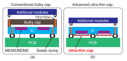
Vacuum and hermetic packaging is a critical requirement for optimal performance of many micro-electromechanical systems (MEMS), vacuum electronics, and quantum devices. However, existing packaging solutions are either elaborate to implement or rely on bulky caps and footprint-consuming seals. Here, we address this problem by demonstrating a waferlevel vacuum packaging method featuring transfer bonding of 25-µm-thin silicon (Si) caps that are transferred from a 100-mm-diameter silicon-on-insulator (SOI) wafer to a cavity wafer to seal the cavities by gold–aluminum (Au–Al) thermocompression bonding at a low temperature of 250 ℃. The resulting wafer-scale sealing yields after wafer dicing are 98% and 100% with sealing rings as narrow as 6 and 9 µm, respectively. Despite the small sealing footprint, the Si caps with 9-µm-wide sealing rings demonstrate a high mean shear strength of 127 MPa. The vacuum levels in the getter-free sealed cavities are measured by residual gas analysis to be as low as 1.3 mbar, based on which a leak rate smaller than 2.8 × 10⁻¹⁴ mbarL/s is derived. We also show that the thickness of the Si caps can be reduced to 6 µm by post-transfer etching while still maintaining excellent hermeticity. The demonstrated ultra-thin packages can potentially be placed in between the solder bumps in flflip–chip interfaces, thereby avoiding the need of through-capvias in conventional MEMS packages.
To realize wafer-level encapsulation with thin caps, two main types of packaging approaches have been developed: vacuum packaging by thin film deposition and wafer bonding of caps. Thin film deposition typically uses a sacrificial layer to cover the structures to be sealed, followed by a cap film deposition. The sacrificial layer is subsequently removed by etching through access holes or by thermal decomposition. Finally, a sealing film is conformally deposited over the cap film to seal the access holes . The total thickness of the capping film stack is usually only a few micrometers, which offers very low profile as well as small footprint seal in the lateral dimension. However, there are several drawbacks associated with this approach . First, the packaging process is complex, especially if MEMS or NEMS movable structures must also be released, since in this case multiple sacrificial layers have to be incorporated. Second, because all the processes must be compatible with the specific device structures and materials, this approach suffers from lack of flexibility and universality. Third, in the case of sacrificial and sealing films made of silicon oxide, silicon nitride, or poly-silicon, the deposition processes typically involve high temperatures, which may hinder its use for many applications, e.g. sealing of MEMS on ICs. In contrast, hermetic sealing of devices by bonding caps on top of the devices is a more versatile approach. Since the preparation of the caps is separated from the preparation of the devices to be sealed, and because various material systems for the bonding and sealing process can be employed, this approach overcomes the abovementioned drawbacks of sealing by thin film deposition.
Another wafer bonding-based approach for sealing of devices with thin caps is realized by Au-Au thermocompression bonding or Au-Sn eutectic bonding of a silicon cap wafer to a device wafer and subsequent thinning of the Si cap wafer by grinding . Although being an extremely successful packaging approach that is widely used in industry, e.g. for packaging of film bulk acoustic resonator (FBAR) filters , this approach poses potential challenges in realizing uniform ultra-thin cap thickness (e.g. ∼5µm) on wafer-scale without impairing the structural integrity and hermeticity of the seals during the grinding process. The reported Si caps realized with this approach were relatively thick, ranging from 60 µm to 80 µm . Besides, either wide metal sealing rings of 75–100 µm were used , or no details of the package design, sealing process, and resulting long-term hermeticity are described in the literature reports.

Fig1
In summary, to the best of our knowledge, there have been no reports where transferred thin caps (< 30 µm) in combination with small sealing footprints (< 10 µm) provided reliable vacuum sealing of cavities. Here, we present a novel wafer-level packaging process that realizes vacuum sealing of cavities using 25 µm-thick Si caps transferred from an SOI wafer. We used the Si device layer of an SOI wafer in our work because of the precise control of the thin Si device layer for the pre-defined caps, the excellent mechanical strength and low residual stress of single-crystalline Si, and the minimal thermal mismatch between the Si caps and typical MEMS device wafers. Compared to the abovementioned postthinning technique by grinding of the bonded Si caps, our approach avoids potential mechanically-induced damage of the caps and sealing rings, if ultra-thin caps are to be achieved. The vacuum sealing is provided by Au-Al thermo-compression bonding at a low temperature of 250 ℃, thus being compatible with standard IC processes. The use of thin single crystalline Si caps in combination with narrow metal sealing rings (< 10 µm) aims to provide a reliable and space-efficient solution for fully hermetic packaging of MEMS and NEMS, and potentially for high-density 3D integration with ICs. Furthermore, the hermeticity of the sealed cavities and the strength of the bonds are evaluated. Finally, the influence of sealing ring width on the resulting sealing yield and the possibility of encapsulating cavities of various dimensions using the thin Si caps are investigated.
下一篇: 化合物半导体的异质集成