The ability to tailor compound semiconductors and to integrate them onto foreign substrates can lead to superior or novel functionalities with a potential impact on various areas in electronics, optoelectronics, spintronics, biosensing, and photovoltaics. This review provides a brief description of different approaches to achieve this heterogeneous integration, with an emphasis on the ion-cut process, also known commercially as the Smart-CutTM process. This process combines semiconductor wafer bonding and undercutting using defect engineering by light ion implantation. Bulk-quality heterostructures frequently unattainable by direct epitaxial growth can be produced, provided that a list of technical criteria is fulfilled, thus offering an additional degree of freedom in the design and fabrication of heterogeneous and flexible devices. Ion cutting is a generic process that can be employed to split and transfer fine monocrystalline layers from various crystals. Materials and engineering issues as well as our current understanding of the underlying physics involved in its application to cleaving thin layers from freestanding GaN, InP, and GaAs wafers are presented.
In his recent analysis of the nature of technology, Arthur proposed that all technologies descend from preexisting ones, so the essence of technological progress is based on assembling new combinations of earlier and refined technologies. This concept of combinatorial evolution, as coined by Arthur, is pertinent to the subject of this review, the heterogeneous integration of compound semiconductors (CSs) by wafer bonding and thin-layer transfer. The possibility of incorporating CS-based devices into the traditional Si technologies has sparked a surge of interest motivated by the novel and improved functionalities potentially achievable by this heterointegration. In this landscape, the much higher charge carrier mobility (as compared with that of Si) and the efficient emission of light by some CSs due to their direct bandgap (as compared with the indirect bandgap of Si) have been the two major driving forces in the development of heterogeneous devices.
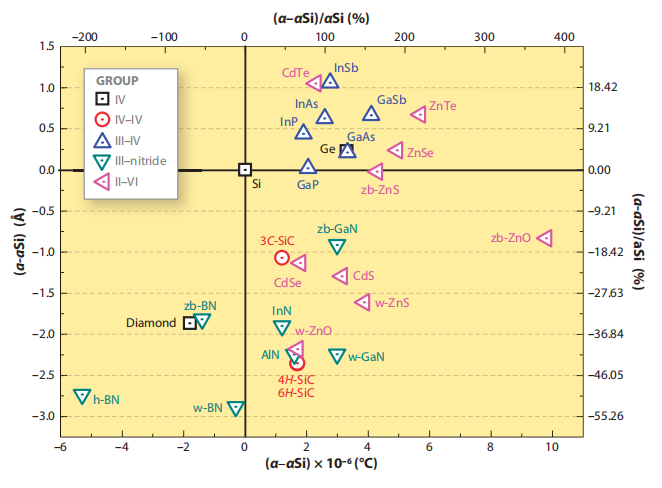
For approximately a half-century, device downscaling was the most important strategy for performance enhancement in Si metal-oxide-semiconductor field effect transistors (MOSFETs). However, keeping with this relentless course of miniaturization turns out to be very challenging for the future technology nodes. This is clearly evidenced in the 2007 edition of the International Technology Roadmap for Semiconductors (ITRS), which establishes the technological challenges in the semiconductor industry. For instance, to meet the performance and power requirements for highly scaled MOSFETs at and below the 10-nm gate length, quasi-ballistic operation with enhanced thermal carrier velocity and injection at the source end appears to be necessary. Ultimately, the introduction of new device structures such as high-transport Ge or CS channels on Si may be needed. As shown in Table 1 , several CSs have a substantially higher electron mobility compared with Si. This has inspired the development of several non-Si transistors. Starting from the mid-1960s, GaAs was the first CS to be used in the fabrication of MOSFETs . Several CSs such as InP, GaAs, GaN, and their ternary and quaternary alloys (InGaAs, InAlAs, AlGaN, InGaP, InGaAsN, AlGaAs, and GaAsSb) as well as SiGe alloys have been used in the fabrication of heterojunction bipolar transistors . Besides GaAs, GaN and InAs have attracted a great deal of attention in the fabrication of high-electron-mobility transistors (HEMTs). In a more recent development, Intel researchers revealed a novel ultrahigh-speed transistor based on InSb quantum wells on GaAs . In spite of the fact that the advantages of CS devices over their Si counterparts were recognized several decades ago, CSs combined with Si were included only in the 2003 and later editions of the ITRS. This is due to the increasing necessity of incorporating non-Si materials into complementary metal-oxide-semiconductor (CMOS) transistors to boost their performance and to enhance their energy efficiency.

Fig1
Another epitaxial variety for the heterogeneous integration is the growth of self-assembled CS nanowires on Si. Among all synthesis methods, the vapor-liquid-solid (VLS) process is the most successful in generating high densities of monocrystalline nanowires . In this process, the growth of nanowires is accomplished via a liquid-metal cluster that acts catalytically as the energetically favored site for vapor-phase reactant absorption and, when saturated, as the nucleation site for crystallization and one-dimensional growth. In the early 1990s, Hiruma and coworkers were the first to demonstrate the growth of GaAs and InAs nanowires via the VLS process, using Au as a catalyst. Recently, several groups reported the growth of defect-free monocrystalline CS nanowires on Si . Although self-assembled nanowires permit the circumvention of lattice and thermal mismatch issues faced in engineered heteroepitaxial layers, it is still premature to predict whether their integration can be successfully achieved at the device level due to numerous difficulties involving control over the size, position, distribution, and orientation of the growing nanowires in addition to the same aforementioned problems faced in CS thin-film device–related processing.
The combination of dissimilar semiconductor materials within the same platform without the need for direct epitaxy can be realized by using wafer bonding and layer transfer technologies. In a first step, the donor and host wafers are tightly joined to form a single entity (92–94). In general, this can be accomplished by following one of the different bonding processes indicated in Figure 2. The bonding process is usually chosen depending on the nature of the initial substrates and their tolerance to temperature as well as on the fifinal application. In principle, a variety of materials can be bonded independently of their structure (monocrystalline, polycrystalline, amorphous), their crystallographic orientation, and their lattice parameter. Due to limited space, we do not address the history and fundamental issues of bonding processes but direct the reader to relevant books and review articles.