We report on the design, fabrication, and characterization of millimeter-length strip waveguides with monolithic grating couplers in commercially available synthetic single-crystal diamond. To minimize the device footprint and the influence of the wafer wedge of the single-crystal diamond thin plate, we adopt a curled waveguide layout. The devices are fabricated using electron-beam lithography and reactive-ion etching. To improve the e-beam patterning accuracy of the grating etch masks, we apply proximity-effect compensation on the gratings and tapers. The linear characterization results indicate a waveguide attenuation of 6.5 dB/mm and a grating transmission of −6.3 dB in the fiber-optic communication C band. These results demonstrate the feasibility of fabricating long waveguides and integrated grating couplers in single-crystal diamond. Our research findings would be beneficial for further exploring quantum and nonlinear optics in integrated single-crystal diamond devices.
Integrated photonic devices have been demonstrated in single-, poly-, and nano-crystal diamond materials . Different fabrication approaches have been used by several research groups worldwide, either relying on electron-beam lithography (EBL) with inductively-coupled plasma reactiveion etching (ICP RIE), or focused-ion-beam (FIB) milling . Compared to FIB milling, the combination of EBL and ICP RIE has the advantage of achieving higher precision and offers the possibility of realizing more sophisticated device designs. Most of the devices realized thus far are fabricated in a layered diamond-on-insulator (DOI) substrate with a diamond membrane on top of a buried oxide (SiO2 ) layer.
To date, the methods used to couple light into and out of single-crystal DOI photonic devices are mainly based on edge coupling , optical fiber taper coupling , or gratingassisted microscope objective coupling. Among the various light coupling approaches, a grating-enabled fiber-tochip coupling method offers a relatively high efficiency and device layout flexibility, as well as the possibility of automated wafer-scale testing. A further advantage is that by integrating monolithic grating couplers in the devices, one avoids additional lithography steps to overlay the diamond waveguides with polymer waveguide extensions required for edge coupling . However, grating couplers optimized for flat-cleaved optical fiber coupling at telecom wavelengths have, to our knowledge, rarely been demonstrated in single-crystal DOI photonic devices. Moreover, the grating couplers recently demonstrated on the aforementioned SCDMW samples featured a relatively low coupling efficiency of −15 dB , which should be futher increased for allowing practical applications.

Fig1
Fabricating integrated devices in poly/nano-crystal DOI substrates is less challenging than in single-crystal DOI substrates, as the former can be prepared by directly growing a diamond layer through plasma-enhanced chemical vapor deposition (PECVD) on an existing wafer-scale SiO2 substrate . The poly/nano-crystal DOI substrates fabricated in such a way do not suffer from wafer wedge. Various high-quality on-chip devices have been realized in poly-crystal DOI substrates, including ring resonators with Q-factors up to 11000, waveguides up to 4.6 mm long with a transmission loss of 5.3 dB/mm, and monolithic grating couplers with a coupling efficiency of −5 dB .
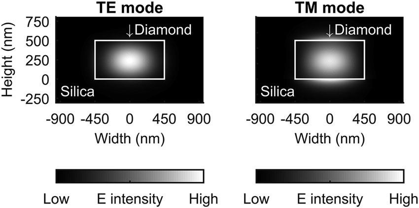
We employ grating couplers to couple the TE polarized light at 1550 nm between the on-chip diamond waveguides and G.652 standard telecom single-mode optical fibers. As the wedged diamond wafer is not suitable for realizing an accurate partiallyetched grating profile, we design a binary grating coupler, with the grating trenches fully etched throughout the diamond layer.
上一篇: 化合物半导体的异质集成