This paper presents the surface/bulk micromachining (SBM) process to allow fabricating released microelectromechanical systems using bulk silicon. The process starts with a (111)-oriented silicon wafer. The structural patterns are defined using the reactive ion etching technique used in surface micromachining. Then the patterns, as well as sidewalls, are passivated with an oxide film, and bare silicon is exposed at desired areas. The exposed bare silicon is further reactive ion etched, which defines sacrificial gap dimensions. The fifinal release is accomplished by undercutting the exposed bulk silicon sidewalls in aqueous alkaline etchants. Because {111} planes are used as etch stops, very clean structural surfaces can be obtained. Using the SBM process, 5-, 10-, and 100-μm-thick arbitrarily-shaped single crystal silicon structures, including comb-drive resonators, at 5-, 30-, and 100- μm sacrificial gaps, respectively, are fabricated. An electrostatic actuation method using p-n junction isolation is also developed in this paper, and it is applied to actuate comb-drive resonators. The leakage current and junction capacitance of the reversedbiased p-n junction diodes are also found to be sufficiently small for sensor applications. The developed SBM process is a plausible alternative to the existing micromachining methods in fabricating microsensors and microactuators, with the advantage of using single crystal silicon.
In surface micromachining, the structural shape is defined by reactive ion etching (RIE), which allows fabricating arbitrary patterns. The most common structural material used in surface micromachining is polysilicon deposited by low-pressure chemical vapor deposition. However, depositing a 2- m-thick film takes several hours or more. Moreover, the material properties of amorphous silicon and polysilicon vary significantly with deposition conditions and postdeposition processes . Thus, accurately controlling the residual stress, stress gradient, and Young’s modulus of polysilicon is difficult. In addition, it is very difficult to grow and control the properties of thick polysilicon films.
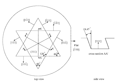
This paper presents a new method for micromachining released structures with single crystal silicon. The developed surface/bulk micromachining (SBM) process utilizes (111) silicon wafers. First, a (111) silicon wafer is reactive ion etched leaving the structural patterns to be released later, and the bulk silicon under the patterns is etched in an aqueous alkaline etchant to release the patterns. In the developed technology, the thickness of the structural layer as well as the thickness of the sacrificial gap are defined by deep silicon RIE. The release of structure is accomplished by aqueous alkaline etching, utilizing the slow etching {111} planes as the etch stop. This results in very smooth and flat bottom surfaces. The required release etch time in a KOH solution, a commonly used alkaline etchant, is comparable to that of etching the sacrificial oxide in HF. The ensuing sections present the complete fabrication method as well as examples of SBM fabricated complex structures, including mesa-island anchored structures and comb-drive resonators.

Fig1
Micromachining with (111) silicon has been attempted previously [16]. However, the structures must be crystallographically aligned to three special directions, and complex structures cannot be fabricated. In addition, the process in [16] requires two photoresist exposure steps that limit the structural thickness. The electrostatic actuation method using junction isolation of single crystal silicon microstructure is reported first in this paper.
上一篇: 考虑光刻中厚掩模效应的边界层模型
下一篇: 一种新型的硅通孔 (TSV) 制造方法