Abstract:This paper aims to realize heterogeneous integrated packaging technology for highintegration by applying a thinning process technology for controlling the thickness of chipsetsused in packaging, i.e., A technology for processing silicon dies with a thickness of 100 um orless and a technology for handling thinning ultrasmall dies. We combine wet etching with dryetching to fit an effective and practical experimental plan. Anisotropic etching in KOHsolutions and ICP etching of silicon die bonding on a glass substrate are investigated. Die withcopper wiring is fabricated and pasted on the substrate to achieve selective etching of thewhole device. The topography of the die surface and corner is analyzed to prevent the influenceon the second layer stacking process.
High-speed Ethernet signal transmission technology is essential in situations where the volume of datatraffic is increasing exponentially, such as data centers, Internet exchange centers, and highperformance servers. To address this problem, heterogeneous integration package technology isfocused on, which can reduce integration and power consumption. Ultra-thin-chip processing andinterconnection (including wafer bonding) through the silicon through holes (TSV) are keytechnologies to implement the heterogeneous integration platform. To realize heterogeneouslyintegrated packaging, the die-thinning of chips is fundamental . The thickness of the silicon waferused as the substrate is reduced, resulting in a thinner device. At the same time, the bandwidth isincreased, and the occupied space is reduced. This thickness thinning can facilitate the implementationof multilayer stacking. Second, it is simple to realize via making and interconnecting in the backend, and it is advantageous for sawing finished devices.
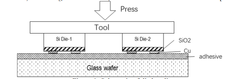
The existing packaging process was executed by die thinning first and then bonding on a substrate.This process is difficult to control when the intermediate die becomes thinner to a certain level duringdie bonding, resulting in a defect in the suction step of lifting the die. In addition, this method islimited because the size of the die varies for heterogeneously integrated packaging. To address thisproblem, the process of thinning the entire sample after bonding was studied.

When NH2OH is added, the etching rate is significantly increased. At 60℃, the etching rate ismultiplied by 23; at 80℃, it is multiplied by 72 because the decomposition of NH2O− and OH− fromNH2OH promotes reaction equilibrium. Surface morphology is essential for determining ifsubsequent encapsulation can be successfully performed. Figure 3 shows the flatness of the etched diesurface. The flatness gradually increases from 40° to 80°, yet the error bar shows between 0.6 and 1um. However, when the temperature approaches 100℃, the flatness will exceed 1 um, and excessivefoaming will eventually affect the flatness. Figure 4 shows the surface of sample and figure 5 showsthe corner angle of the die after wet etching and dry etching. The results show that wet etching is 67°and dry etching is 90° because wet etching is isotropic, and dry etching is anisotropic. So finally, thesurface of the sample forms the same appearance as the figure 4 and figure 5, that is, the edges andcorners will be etched faster than the middle side.
Chip-to-wire and wafer-to-wafer are used to complete bonding and die bonding is the packing stageafter die thinning. However, this wafer-level thinning bonding can only be used for isomorphism. Ifthe wafer thickness is less than 150 um, it will become flexible and fragile, making it difficult tocontrol and lowering the yield. Second, dies with metal wiring cannot be thinned using CMP and otheroperations, as this would destroy the internal structure and cause a short circuit.
上一篇: 自动供液系统(SDS)
下一篇: SiC掺杂剂选择性光电化学蚀刻