Single crystalline 4H-SiC is a wide-gap semiconductor with optical properties that are poised to enable new applications in MEMSand quantum devices. A number of key hurdles remain with respect to the micro and nano-fabrication of SiC to prepare precisephotonic structures with nanometer-scale precision. These challenges include development of a fast, scalable etching process forSiC capable of producing a sub-nanometer roughness semiconductor surface while simultaneously reducing the total thicknessvariation across a wafer. Our investigation into UV photoelectrochemical processing of SiC reveals high dopant-type selectivityand the advantage of multiple etch stops to reduce layer thickness variation. We demonstrate dopant-type selectivities >20:1 usinga single step and a >100x reduction in surface variation by combining two etch stops. Moreover, the etch rate is fast (>4 μm h−1)and the etched surface is smooth (∼1 nm RMS). These results demonstrate a scalable path to the fabrication of precise nanoscaleSiC structures and electronic devices that will enable the next generation of MEMS and photonic quantum devices.
Wide band-gap semiconductors, including aluminum nitride(AlN), gallium nitride (GaN), and silicon carbide (SiC), are usedin commercial devices such as micro-electromechanical systems(MEMS), and high-frequency and high-power electronics. 4H-SiC inparticular has been shown to host defect centers as quantummemories in an integrated photonic platform,1 and the ability toisotopically enhance the material makes the quantum memories in4H-SiC more promising. Its nonlinear optical properties also suggestsignificant application potential for both quantum and classicalphotonics in clocking and wavelength transduction.
We hypothesize that low TTV SiCOI can be prepared by photoelectrochemically etching down to an epitaxial defined dopant layer(which can also be the device layer) as shown in Fig. 1. A dopedepitaxial layer therefore serves as an etch-stop. In this example, the basesubstrate is bulk 4H-SiC with an epitaxial sacrificial layer of doped 4HSiC, followed by the relevant 4H-SiC layers necessary for the finaldevice. Finally, a dielectric, such as silicon oxide (SiO2), is deposited ontop (Fig. 1a). The thickness range of epitaxial grown layers of SiCacross a wafer can be well controlled to within <10% and we expectthis to improve over time. This stack is wafer-bonded to a carriersubstrate (handle wafer) such as Si/SiO2 (Fig. 1b). In the next step themajority of the original SiC substrate is removed by mechanicalgrinding and polishing until the middle of the sacrificial layer is reached(Fig. 1c). Although the mechanical grinding and polishing can yield alocally smooth surface and uniform thickness over small length scales,ranging from micrometers to millimeters, the grinding usually yieldsnon-uniform film thickness compared to a sub-micron thick target filmacross an entire wafer. Mechanical grinding may additionally introducenew lattice defects such as dislocations and crystal strain. Therefore, itis important to stop mechanical grinding in the sacrificial SiC layer(Fig. 1c) where this stopping layer is at least a few micrometers thick.The results presented here demonstrate that dopant selective PECetching of the sacrificial layer(s) can reduce surface variations by >20× for a single step (sacrificial n-type on a p-type etch stop layer) and by>100 × when two sacrificial layers are used to expose a clean,crystalline, low-defect-density, low TTV surface of SiC (Fig. 1d).

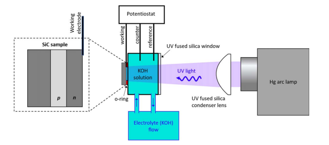
Linear sweep voltammetry (LSV) and chronoamperometry (CA)were used to characterize the electrochemical and PEC processesoccurring on the SiC surface at various potentials. SiC is chemicallystable in 1 wt% KOH with no etching at open circuit (chemical etch)and little-to-no dark current (electrochemical etch) expected whenbiased within a relevant potential window (e.g. −1 to 3 V). In atypical LSV measurement, the applied voltage was swept to positive(anodic) potentials and the resulting current used to determine therate of oxidation (positive current). Anodic sweep measurementswere stopped just after passivation peaks to avoid significant buildup of oxidation products thereby enabling subsequent CA measurements at chosen constant potentials. If needed to remove significantsurface passivation, a cathodic sweep was performed. In extremecases, the sample was removed and the passivation removed byetching with 5 wt% HF. It is worth noting that although LSV can beused to identify a particular reaction and estimate its potential, thesemeasurements are made under dynamic potentials and providelimited information as to how a particular reaction (at a constantpotential) changes over time. Insights into the reaction kinetics/dynamics are gleaned through CA. After characterizing the etchingbehavior with LSV, bulk etching was performed using CA at fixedpotentials chosen from the LSV data.
上一篇: 3D封装中在基板上键合后的管芯级减薄
下一篇: 低温蚀刻过程中涉及的钝化机制