Integrated circuit and other semiconductor fabrication processes are well known in the art. The fabrication of anintegrated circuit chip typically begins with a thin, polishedslice of high-purity, single-crystal semiconductor materialSubstrate (such as silicon or germanium) called a "wafer.which is them processed in a sequence of physical and chemical processing steps to form various circuit structures on thewafer. During the fabrication process, various types of thinfilms may be deposited on the wafer using various techniquesSuch as thermal oxidation to produce silicon dioxide films, chemical vapor deposition to produce silicon, silicon dioxide,and silicon nitride films, and sputtering or other techniques toproduce other metal films. The semiconductor structure ismodified by applying masks, dopants, deposition processes,and etch processes, as known to those of skill in the art.0003 Vacuum processing chambers are often used foretching and chemical vapor deposition (CVD) of materials onSubstrates by Supplying an etching or deposition gas to thevacuum chamber and application of a radio frequency (RF)field to the gas to energize the gas into a plasma state. However, in plasma processing of wafers, process drift (i.e., thechange of process performance over a certain amount of time)can occur, and conventional processes and apparatuses canresult in a varying etch rate and a great amount of polymer build up.
The present disclosure an embodiment that includesan apparatus with an edge ring configured to Surround aperimeter of a semiconductor wafer in a semiconductor process, the edge ring having a plurality of protrusions located onan upper Surface of the edge ring, the protrusions capable ofpreventing the semiconductor wafer from moving outside thebounds of a process plane.
Another embodiment describes an apparatus havinga semiconductor process chamber and an electrostatic chuckdisposed within the semiconductor process chamber. Theapparatus also includes a semiconductor wafer Supported bythe electrostatic chuck; and an edge ring, the edge ring havinga plurality of protrusions located on an upper Surface of theedge ring, the protrusions capable of preventing the semiconductor wafer from moving outside the bounds of a process plane.

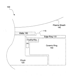
Fig1
While the making and using of various embodiments of the present disclosure are discussed in detail below, it should be appreciated that the present disclosure providesmany applicable inventive concepts, which can be embodiedin a wide variety of specific contexts. Although described inrelation to such apparatus and methods, the teachings andembodiments of the present disclosure may be beneficially implemented with a variety of manufacturing and applications. The specific embodiments discussed herein are, therefore, merely demonstrative of specific ways to make and usethe disclosure, and do not limit the scope of the disclosure.
One function of edge ring 110 relates to its effect onprocess uniformity across the substrate. It is well known thatthe equipotential lines of the plasma sheath 140 curve upwardsharply past the edge of the chuck 120. Without an edge ring 110, the wafer edge electrically defines the outer edge of thechuck, and the equipotential lines would curve upwardsharply in the vicinity of the wafer edge. As such, areas of thewafer around the wafer edge would experience a differentplasma environment from the plasma environment that existsat the center of substrate, thereby contributing to poor processuniformity across the Substrate Surface.