Through-Silicon-Vias (TSV) are the key to 3Dintegrated microsystems. Their fabrication leads to reliabilityissues linked to the thermo-mechanical stress induced in the siliconaround the vias. In this work, we propose to reduce the siliconresidual stress in high aspect ratio copper TSVs (HAR TSV) usingan electrografted polymer insulator, poly-4-vinylpyridine (P4VP),in replacement of the traditional silicon oxide layer. We useRaman spectroscopy to make the first investigation of the residualstress in the Si around P4VP insulated TSVs and compare it toSiO2 insulated TSVs. The results show that P4VP acts as a stressbuffer layer because of its particular mechanical properties as themeasured residual stress in Si is significantly reduced at roomtemperature around the polymer insulated HAR TSVs. Thepotential benefits of such a technology are not only a betterthermo-mechanical reliability of 3D integrated microsystem, butalso a greater integration density.
This is one of the main technological challenge one faces tointegrate Cu TSVs in the microsystem fabrication process flowthat impact significantly the layout optimization. Indeed, whiletransistor placement is forbidden within a significant keep-outzone (KOZ) around each TSV, the area above the TSV is alsooften forbidden to interconnections for mechanical integrityreasons. The KOZ defines the minimum distance between twoTSy to ensure the mechanical reliability of the microsystem.and the minimum distance between a TSV and an active deviceto minimize the impact on the carrier mobility. Electrical KOZis defined based on a 7% mobility change or an equivalent stressof 100 MPa [9] (some state a 5 % mobility change [7]).Moreover, the Si stress around a TSV is proportional to thesquare of the TSV radius (9]. Thus, scaling down TSVs to fewmicrometers radius openings can significantly reduce the Siresidual stress, along with a gain of' real estate in the design.
We have been studying an innovative technology forinsulating TSVs based on the electrografting of an organicpolymer, poly 4-vinylpyridine (P4VP) [14] [17]. Indeed, theP4VP electrografting process has shown promising results toinsulate high aspect ratio copper TSVs in Vial-[ast for the 3Dintegration of an imaging system (17]. This process is of interestas it provides an interesting alternative to SiO, based materialsfor high aspect ratio copper TSVs insulation in 3D integrationprocess flow. Copper TSVs cannot be metallized in Via-First asthe Front End Of Line requires high temperature processes thatcause the copper filling to diffuse into the silicon substrate (18].The deposition of SiO, based dielectric is thus limited toChemical Vapor Deposition based methods, which are costly toimplement to obtain a conformal and uniform layer in such deepand narrow structures. On the contrary in the same conditionsof' integration, the electrografted polymer film is highlyconformal and uniform, easy to implement and shows similardielectric film properties than that of SiO2 [l5].
We conclude that, if existing, the stress close to the P4VPinsulated TSV edge is considerably lower compared to SiOpinsulated TSVs. This observation is of great interest, as itclearly shows that with the use of the electrografted p4VP, theresidual Si stress at the edges of the TSV is dramaticallyreduced compared to SiO, insulated TSVs.
The metallization process of the TSV includes a 250°Cannealing step after the filling with Cu. This temperature isabove the expected glass transition temperature of p4VP below200°C, relatively close to its bulk value [42], [43]. Ourhypothesis is that 7, is reached during the final annealing of theTSV. Even if the polymer is confined between the Cu fillingand the Si substrate, the polymer's chains can reconfigurebetween reticulation points: there is a viscoelastic relaxation ofthe stress through self-reorganization of the P4VP chains. Thepolymer would therefore act as a buffer layer and reconfigureitself to absorb the stress. After cool down, once below 1, themechanisms that lead to stress in TSV come into play again.This occurring at a lower temperature than that common to SiOpprocess, we expect the residual stress to be lower and furtherreduced by the low Young's modulus of P4VP.

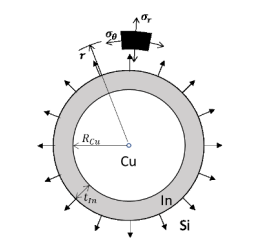
Fig1
The authors would like to thank, S. Ecoffey, C. Mireault and J.Plathier for their contribution. This work was performed at theUniversite de Sherbrooke, the Institut National de la RechercheScientifique (INRS) and MiOro Innovation CollaborativeCenter (C2Ml) supported by grants from the Natural Sciencesand Engineering Research Council of Canada (NSERC).PRIMA.MITACS and PROMPT. We thank ourindustrialcollaborators Teledyne DALSA Semiconductor and aveni. Wefinally thank the reviewers for their contributions at improvingthe completeness of this paper.