The concept of miniaturization wasintroduced because of advancement in science andtechnology during 1980s. These miniaturizedstructures and designs are of high significance formaking up with the macroscopic technology, for thesake of interfacing with microscopic world. Thefabrication of micro structures and designs which arethe advanced applications of micro fabrication areused for the process of micromachining structures inthree dimensions as it is essential for interfacing withthe nanotechnology. Micromachining which meansperforming cutting or grinding operations or selectiveremoval of wafer to produce various structures hasmuch important applications like accelerometerswhich are used to trigger air bags in cars. Thelithography and etching processes are used to shapethe bulk materials into microstructures in microfabrication mechanism. Different ion bombardmenttechniques and chemical reactive mechanisms areused for a type of etching which is carried out invacuum chamber, whereas chemical solutions areused for another type of etching mechanism whoseprocedures are finished in a bath. This surveyillustrates different etching methodologies and theimpact of various etchants in wet etching.
There are a lot of processing steps in the process ofmicro fabrication. Etching is an important step in theprocess of micro fabrication. The term etching refers tothe removal of layers from the surface of wafer whenmanufacturing. This is a critically important process, each and every wafer undergo a lot of etching process.The material which is used to protect the wafer from theetchants is known as the masking material, which is usedin many etching steps to resist etching. This maskingmaterial can be a photoresist and it is patterned usingphotolithography.Etching can also be referred as makingcavities and these cavities should have specific depthaccording to the purposes. The depth of such cavitiesproduced can be controlled by etching time and theetching rate. The success in performing etchingmechanism is that, the top layer of a multilayer structureshould be removed entirely, without any kind of damagein the underlying layers or the masking layers. Thisentirely depends on the ratio of the etch rates of twomaterials which is termed as selectivity. During somecases of etching, etches undercut the mask layer and itproduces sloping sidewalls forming cavities. Thedistance of undercutting is called bias.
Fundamental etching techniques used in microfabrication are dry etching (plasma phase) and wetetching (liquid phase). The disadvantages of dry etchingare as follows, the gases used in dry etching are quitetoxic and corrosive. It requires redeposition of nonvolatile compounds and it needs specialized andexpensive equipment.
Wet etching is inexpensive and it has been extensivelyused for the fabrication of MEMS components such asdiaphragms based on single crystal silicon, especially on(100) water and cantilever beam.Wet etching is theprocess of removing a material by using liquid chemicalsor etchants from a wafer. The specific patterns aredefined by masks on the wafer. Materials that are notprotected by the masks are etched away by liquidchemicals. These masks are deposited and patterned onthe wafers using lithography. Wet etching processinvolves multiple chemical reactions that consume theoriginal reactants and produce new reactants.
Wet etchants are often isotropic and they lead to largerbias during the etching of thick films. They also requiredisposal of large amounts of toxic waste. This etchmethod is particularly effective just before "backend"processing (BEOL), where wafers are normally very thinafter wafer backgrinding and are very sensitive tothermal or mechanical kind of stress. Etching a muchthin layer of few micrometers will remove micro cracksproduced during back grinding resulting in the waferhaving dramatically increased strength and flexibility.This type of etching is quick, easy and cheap. Roundingof sharp anisotropic corners is used to avoid stressconcentration. This exhibits same etch rate in alldirections. Lateral etch rate is about as same as thevertical etch rate. This etch rate never depends on theorientation of the mask edge.
For isotropic wet etching, a mixture of hydrofluoric acid,nitric acid, and acetic acid (HNA) is the most commonetchant solvent for silicon [1]. The concentrations ofeach etchant determines the etch rate. Silicon dioxide orsilicon nitride is often used as a masking material againstHNA. When the reaction occurs, material is removedlaterally at a rate similar to the speed of downwardetching. Wet chemical etching is generally isotropic eventhough a mask is present since the liquid etchant canpenetrate underneath the mask. If the directionality isofmuch importance for high-resolution pattern transfer,process of wet chemical etching is normally prohibited.
This is also known as Orientation Dependent Etching.Liquid etchants etch crystalline materials at differentrates depending upon which crystal face is exposed toetchant used. A large difference in the etch rate is theredepending on the silicon crystalline plane. When siliconlike materials are used, this effect can allow very highanisotropy.
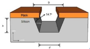
The key technique for the fabrication of variousmicromechanical devices is anisotropic etching. The etchrate (ER) in anisotropic etching is much faster in etchingplane as etch time progress usually the (111) planes ofsilicon. The important factor of anisotropy etchingincludes selectivity, handling and process compatibilityand anisotropic. Anisotropic wet etching produces atypical etch rate about 1µm/min.

Fig1
The orientation of the crystals is one of the prime factorsthat affect etching. There are a lot of cases where themechanism of etching gets affected because of thecrystal orientations.The concept of Miller Indices is veryimportant for this study about the orientation of crystal asit is used to specify the directions and planes. Thesedirections and planes could be in lattices or in crystals.The number of indices will match with the dimension ofthe lattice or the crystal. The importance of the millerindices is that, in Materials Science it is important tohave a notation system for atomic planes since theseplanes influence the Optical properties, reactivity ofmaterial, Surface tension and dislocations.The etch ratesdiffer for different crystal orientations which are knownto us by the concept of miller indices.
The hillocks [4-8] were bounded by (111) crystal planes.The dependences of the (110) etch rates shows a similartendency to those of the (100) plane. The etch rates arehigher than those for the (100) plane. As theconcentration increases, the smoothness of the etched(100) surface changed. Etching of silicon(110) surfacerevealed that at 10 wt %, the surface was covered by anirregular pattern and a ridged pattern in the <110>direction.